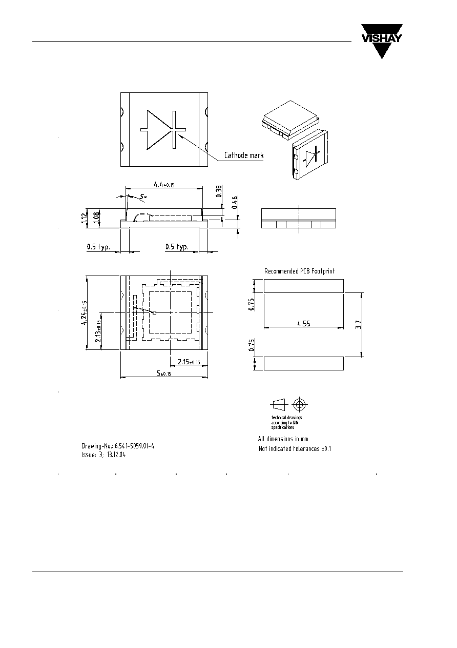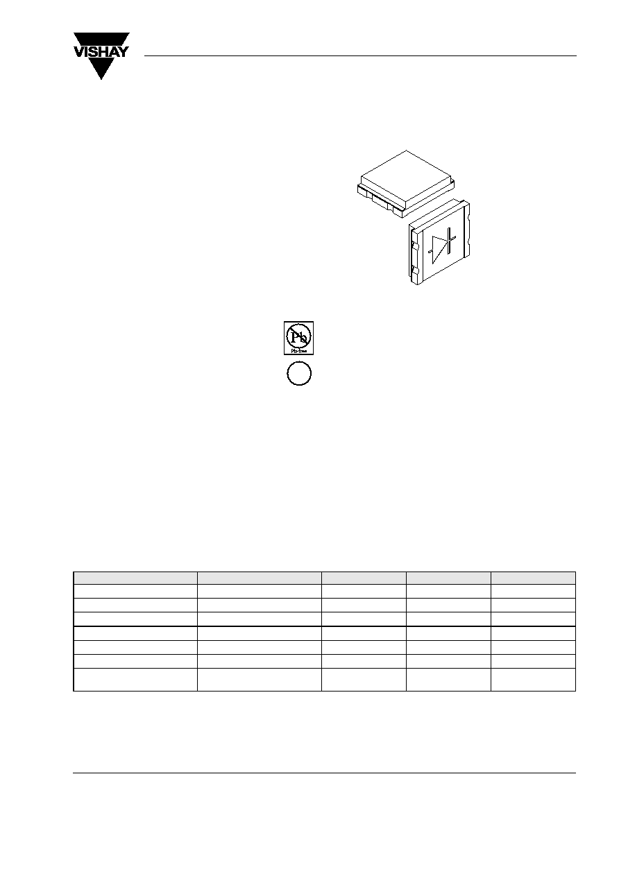
TEMD5020
Document Number 84685
Rev. 1.0, 08-Mar-05
Vishay Semiconductors
www.vishay.com
1
Silicon PIN Photodiode
Description
TEMD5020 is a high speed and high sensitive PIN
photodiode. It is a miniature Surface Mount Device
(SMD) including the chip with a 5.7 mm
2
sensitive
area, detecting visible and near infrared radiation.
Features
· Radiant sensitive area (A = 5.7 mm
2
)
· Wide angle of half sensitivity
= ± 65 °
· High photo sensitivity for visible and near
infrared radiation
· Fast response times
· Small junction capacitance
· Plastic package
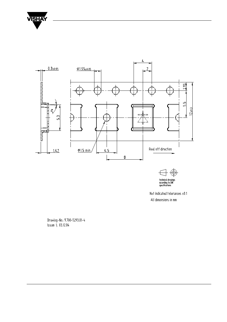
· Floor life 72 h (MSL 4, acc. J-STD-20)
· Lead-free component
· Component in accordance to ELV 2000/53/EC,
RoHS 2002/95/EC and WEEE 2002/96/EC
Applications
High speed photo detector
Absolute Maximum Ratings
T
amb
= 25 °C, unless otherwise specified
Parameter
Test condition
Symbol
Value
Unit
Reverse Voltage
V
R
60
V
Power Dissipation
T
amb
25 °C
P
V
215
mW
Junction Temperature
T
j
100
°C
Operating Temperature Range
T
amb
- 40 to + 100
°C
Storage Temperature Range
T
stg
- 40 to + 100
°C
Soldering Temperature
t
3 s
T
sd
260
°C
Thermal Resistance Junction/
Ambient
R
thJA
350
K/W
e4
www.vishay.com
2
Document Number 84685
Rev. 1.0, 08-Mar-05
TEMD5020
Vishay Semiconductors
Electrical Characteristics
T
amb
= 25 °C, unless otherwise specified
Optical Characteristics
T
amb
= 25 °C, unless otherwise specified
Typical Characteristics
(Tamb = 25
°C unless otherwise specified)
Parameter
Test condition
Symbol
Min
Typ.
Max
Unit
Forward Voltage
I
F
= 50 mA
V
F
1
1.3
V
Breakdown Voltage
I
R
= 100
µA, E = 0
V
(BR)
60
V
Reverse Dark Current
V
R
= 10 V, E = 0
I
ro
2
30
nA
Diode capacitance
V
R
= 0 V, f = 1 MHz, E = 0
C
D
48
pF
Parameter
Test condition
Symbol
Min
Typ.
Max
Unit
Open Circuit Voltage
E
e
= 1 mW/cm
2
,
= 950 nm
V
o
350
mV
Temp. Coefficient of V
o
E
e
= 1 mW/cm
2
,
= 950 nm
TK
Vo
-2.6
mV/K
Short Circuit Current
E
e
= 1 mW/cm
2
,
= 950 nm
I
k
32
µA
Temp. Coefficient of I
k
E
e
= 1 mW/cm
2
,
= 950 nm
TK
Ik
0.1
%/K
Reverse Light Current
E
e
= 1 mW/cm
2
,
= 950 nm,
V
R
= 5 V
I
ra
25
35
µA
Angle of Half Sensitivity
± 65
deg
Wavelength of Peak Sensitivity
p
900
nm
Range of Spectral Bandwidth
0.5
600 to 1050
nm
Noise Equivalent Power
V
R
= 10 V,
= 950 nm
NEP
4 x 10
-14
W/
Hz
Rise Time
V
R
= 10 V, R
L
= 1 k
, = 820 nm
t
r
100
ns
Fall Time
V
R
= 10 V, R
L
= 1 k
, = 820 nm
t
f
100
ns
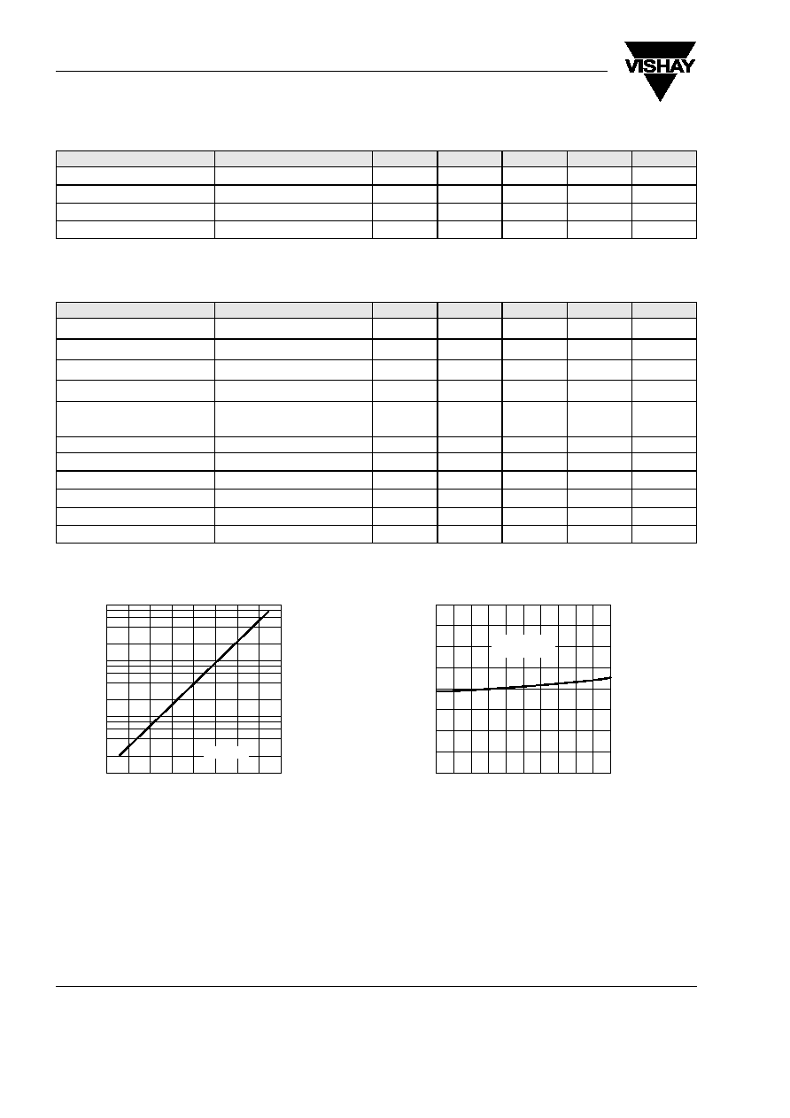
Figure 1. Reverse Dark Current vs. Ambient Temperature
20
40
60
80
1
10
100
1000
100
94 8403
V
R
= 10 V
I
-
Reverse
Dark
Current
(
n
A
)
ro
T
amb
- Ambient Temperature (
°C )
Figure 2. Relative Reverse Light Current vs. Ambient Temperature
0.6
0.8
1.0
1.2
1.4
94 8409
I
-
Rel
a
tive
Reverse
Light
Current
r
a
rel
V
R
= 5 V
= 950 nm
T
amb
- Ambient Temperature (
°C )
100
80
60
40
20
0
TEMD5020
Document Number 84685
Rev. 1.0, 08-Mar-05
Vishay Semiconductors
www.vishay.com
3
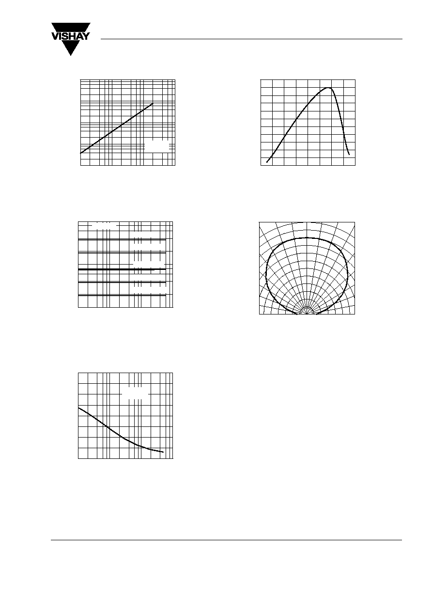
Figure 3. Reverse Light Current vs. Irradiance
Figure 4. Reverse Light Current vs. Reverse Voltage
Figure 5. Diode Capacitance vs. Reverse Voltage
0.01
0.1
1
0.1
1
10
100
1000
I
Reverse
Light
Current
(
µ
A)
ra
E
e
Irradiance ( mW/ cm
2
)
10
94 8421
V
R
= 5 V
= 950 nm
0.1
1
10
1
10
100
V
R
Reverse Voltage ( V )
100
94 8422
I
Reverse
Light
Current
(
µ
A)
ra
1 mW/cm
2
0.5 mW/cm
2
0.2 mW/cm
2
0.1 mW/cm
2
0.05 mW/cm
2
= 950 nm
0.1
1
10
0
20
40
60
80
C
Diode
Capacitance
(
p
F
)
D
V
R
Reverse Voltage ( V )
100
94 8423
E=0
f=1MHz
Figure 6. Relative Spectral Sensitivity vs. Wavelength
Figure 7. Relative Radiant Sensitivity vs. Angular Displacement
350
550
750
950
0
0.2
0.4
0.6
0.8
1.0
1150
94 8420
S(
)
Relative
Spectral
Sensitivity
rel
Wavelength ( nm )
0.4
0.2
0
0.2
0.4
S
Relative
Sensitivity
rel
0.6
94 8406
0.6
0.9
0.8
0°
30°
10
°
20
°
40°
50°
60°
70°
80°
0.7
1.0