
TL393, TL393Y
DUAL DIFFERENTIAL COMPARATORS
SLCS120A ş AUGUST 1993 ş REVISED DECEMBER 1993
1
POST OFFICE BOX 655303
Ě
DALLAS, TEXAS 75265
D
Low-Voltage and Single-Supply Operation
V
CC
= 2 V to 7 V
D
Common-Mode Voltage Range That
Includes Ground
description
The TL393 is a dual differential comparator built using a new Texas Instruments-developed bipolar process. The
TL393 is intended as an enhanced alternative to the industry-standard LM393 in circuits with supply-voltage
limits of 7 V.
The new bipolar process allows the TL393 to perform with lower supply-current requirements than the LM393
(0.7 mA typical) while still providing a faster response time than the older device.
Package availability for this device includes the TSSOP (thin-shrink small-outline package). With a maximum
thickness of 1.1 mm and a package area that is 25% smaller than the standard surface-mount package, the
TSSOP is ideal for high-density circuits, particularly in hand-held and portable equipment.
AVAILABLE OPTIONS
SUPPLY
RESPONSE TIME
PACKAGED DEVICES
CHIP FORM
TA
CURRENT
(TYP)
RESPONSE TIME
(TYP)
SMALL OUTLINE
(D)
PLASTIC DIP
(P)
TSSOP
(PW)
CHIP FORM
(Y)
ş 40
░
C to 105
░
C
0.7 mA
0.65
Á
s
TL393ID
TL393IP
TL393IPWLE
TL393Y
The PW packages are only available left-ended taped and reeled (e.g., TL393IPWLE).
symbol (each comparator)
OUT
IN+
IN ş
Copyright
ę
1993, Texas Instruments Incorporated
PRODUCTION DATA information is current as of publication date.
Products conform to specifications per the terms of Texas Instruments
standard warranty. Production processing does not necessarily include
testing of all parameters.
1
2
3
4
8
7
6
5
1OUT
1IN ş
1IN+
GND
V
CC
2OUT
2IN ş
2IN+
D, P, OR PW PACKAGE
(TOP VIEW)
TL393, TL393Y
DUAL DIFFERENTIAL COMPARATORS
SLCS120A ş AUGUST 1993 ş REVISED DECEMBER 1993
2
POST OFFICE BOX 655303
Ě
DALLAS, TEXAS 75265
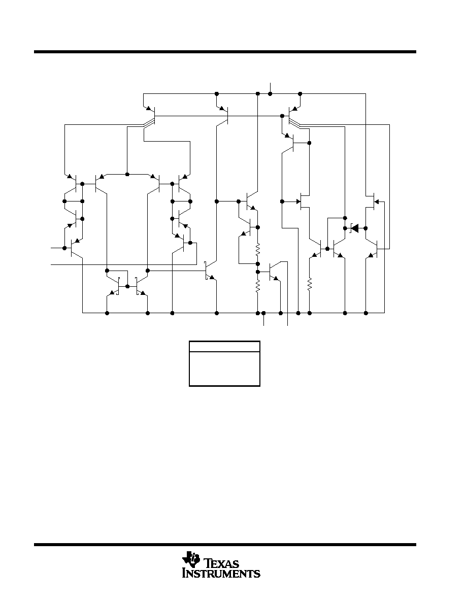
equivalent schematic (each comparator)
VCC
GND
OUT
IN +
IN ş
COMPONENT COUNT
Transistors
48
Resistors
5
Diodes
E i FET
7
2
Epi-FETs
2
TL393, TL393Y
DUAL DIFFERENTIAL COMPARATORS
SLCS120A ş AUGUST 1993 ş REVISED DECEMBER 1993
3
POST OFFICE BOX 655303
Ě
DALLAS, TEXAS 75265
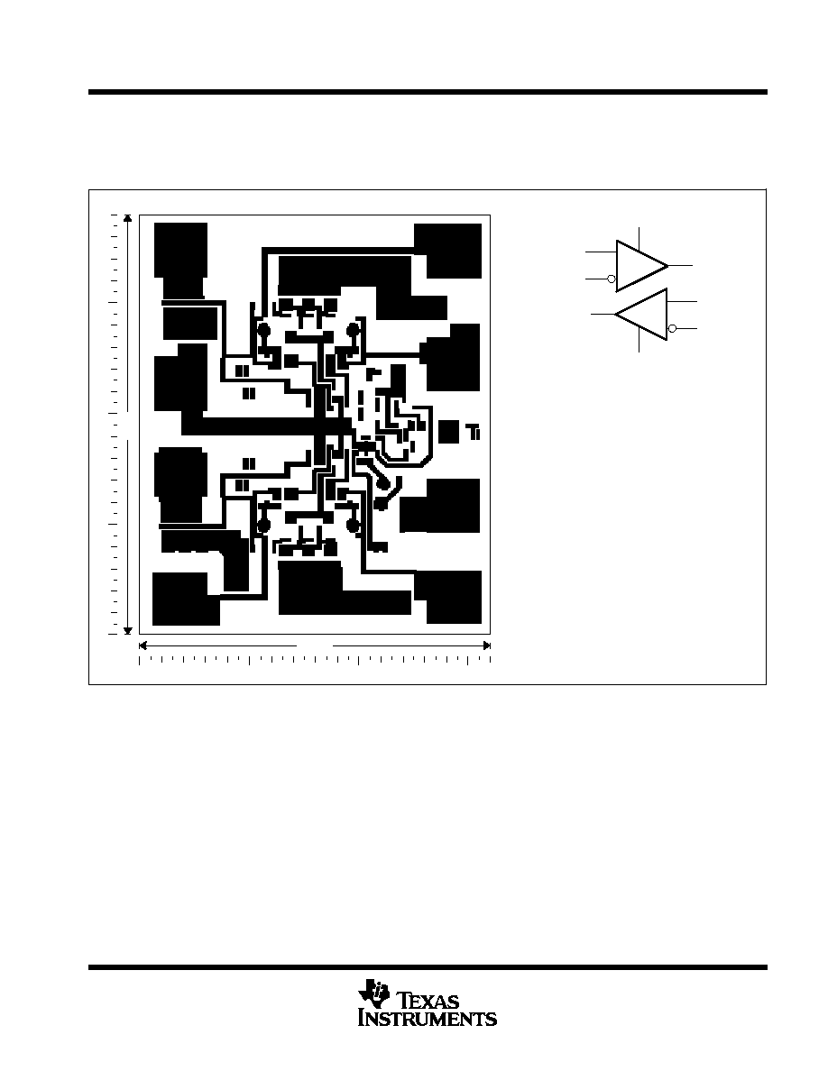
TL393Y chip information
This chip, when properly assembled, displays characteristics similar to the TL393. Thermal compression or
ultrasonic bonding may be used on the doped-aluminum bonding pads. Chips may be mounted with conductive
epoxy or a gold-silicon preform.
BONDING PAD ASSIGNMENTS
CHIP THICKNESS: 13 TYPICAL
BONDING PADS: 3.54
Î
3.54 MINIMUM
TJmax = 150
░
C
TOLERANCES ARE
▒
10%.
ALL DIMENSIONS ARE IN MILS.
PIN (4) IS INTERNALLY CONNECTED
TO BACKSIDE OF CHIP.
+
ş
1OUT
1IN +
1IN ş
VCC
(8)
(6)
(3)
(2)
(5)
(1)
ş
+
(7)
2IN +
2IN ş
2OUT
(4)
GND
32
38
(1)
(2)
(3)
(4)
(5)
(6)
(7)
(8)

TL393, TL393Y
DUAL DIFFERENTIAL COMPARATORS
SLCS120A ş AUGUST 1993 ş REVISED DECEMBER 1993
4
POST OFFICE BOX 655303
Ě
DALLAS, TEXAS 75265
absolute maximum ratings over operating free-air temperature range (unless otherwise noted)
Supply voltage, V
CC
(see Note 1)
7 V
. . . . . . . . . . . . . . . . . . . . . . . . . . . . . . . . . . . . . . . . . . . . . . . . . . . . . . . . . . . . .
Differential input voltage, V
ID
(see Note 2)
7 V
. . . . . . . . . . . . . . . . . . . . . . . . . . . . . . . . . . . . . . . . . . . . . . . . . . . . .
Input voltage, V
I
(any input)
7 V
. . . . . . . . . . . . . . . . . . . . . . . . . . . . . . . . . . . . . . . . . . . . . . . . . . . . . . . . . . . . . . . . . .
Output voltage, V
O
7 V
. . . . . . . . . . . . . . . . . . . . . . . . . . . . . . . . . . . . . . . . . . . . . . . . . . . . . . . . . . . . . . . . . . . . . . . . . .
Output current, I
O
(each output)
20 mA
. . . . . . . . . . . . . . . . . . . . . . . . . . . . . . . . . . . . . . . . . . . . . . . . . . . . . . . . . . .
Duration of short-circuit current to GND (see Note 3)
unlimited
. . . . . . . . . . . . . . . . . . . . . . . . . . . . . . . . . . . . . . .
Continuous total dissipation
See Dissipation Rating Table
. . . . . . . . . . . . . . . . . . . . . . . . . . . . . . . . . . . . . . . . . . .
Operating free-air temperature range, T
A
ş 40
░
C to 105
░
C
. . . . . . . . . . . . . . . . . . . . . . . . . . . . . . . . . . . . . . . . . . .
Storage temperature range
ş 65
░
C to 150
░
C
. . . . . . . . . . . . . . . . . . . . . . . . . . . . . . . . . . . . . . . . . . . . . . . . . . . . . . . .
Lead temperature 1,6 mm (1/16 inch) from case for 10 seconds
260
░
C
. . . . . . . . . . . . . . . . . . . . . . . . . . . . . . .
Stresses beyond those listed under "absolute maximum ratings" may cause permanent damage to the device. These are stress ratings only, and
functional operation of the device at these or any other conditions beyond those indicated under "recommended operating conditions" is not
implied. Exposure to absolute-maximum-rated conditions for extended periods may affect device reliability.
NOTES:
1. All voltage values, except differential voltages, are with respect to network GND.
2. Differential voltages are at IN+ with respect to IN ş.
3. Short circuits from the outputs to VCC can cause excessive heating and eventual destruction of the chip.
DISSIPATION RATING TABLE
PACKAGE
TA
25
░
C
POWER RATING
DERATING FACTOR
ABOVE TA = 25
░
C
TA = 70
░
C
POWER RATING
TA = 85
░
C
POWER RATING
D
725 mW
5.8 mW/
░
C
464 mW
377 mW
P
1000 mW
8.0 mW/
░
C
640 mW
520 mW
PW
525 mW
4.2 mW/
░
C
336 mW
273 mW
recommended operating conditions
MIN
MAX
UNIT
Supply voltage, VCC
2
7
V
Operating free-air temperature, TA
ş 40
105
░
C
TL393, TL393Y
DUAL DIFFERENTIAL COMPARATORS
SLCS120A ş AUGUST 1993 ş REVISED DECEMBER 1993
5
POST OFFICE BOX 655303
Ě
DALLAS, TEXAS 75265
electrical characteristics, V
CC
= 5 V (unless otherwise noted)
PARAMETER
TEST CONDITIONS
TA
TL393
UNIT
PARAMETER
TEST CONDITIONS
TA
MIN
TYP
MAX
UNIT
VIO
Input offset voltage
VO = 1 4 V
VIC = VICRmin
25
░
C
1.5
5
mV
VIO
Input offset voltage
VO = 1.4 V, VIC = VICRmin
Full range
9
mV
VICR
Common mode input voltage range
25
░
C
0 to
VCC ş 1.5
0 to
VCC ş 1.2
V
VICR
Common-mode input voltage range
Full range
0 to
VCC ş2
V
VOL
Low level output voltage
VID = ş1 V, IOL = 1 mA
25
░
C
70
300
mV
VOL
Low-level output voltage
VID = ş1 V, IOL = 4 mA
Full range
200
700
mV
IIO
Input offset current
VO = 1 4 V
25
░
C
5
50
nA
IIO
Input offset current
VO = 1.4 V
Full range
150
nA
IIB
Input bias current
VO = 1 4 V
25
░
C
ş 40
ş 250
nA
IIB
Input bias current
VO = 1.4 V
Full range
ş 400
nA
IOH
High level output current
VID = 1 V,
VOH = 3 V
25
░
C
0.1
nA
IOH
High-level output current
VID = 1 V,
VOH = 5 V
Full range
100
nA
IOL
low-level output current
VID = ş1 V, VOL = 1.5 V
25
░
C
6
mA
ICCH
High level supply current
VO = VOH
25
░
C
140
200
Á
A
ICCH
High-level supply current
VO = VOH
Full range
300
Á
A
ICCL
Low level supply current
VO = VOL
25
░
C
0.8
1
mA
ICCL
Low-level supply current
VO = VOL
Full range
1.2
mA
Full range is ş 40
░
C to 105
░
C.
switching characteristics, V
CC
= 5 V, C
L
= 15 pF, T
A
= 25
░
C
PARAMETER
TEST CONDITIONS
TL393
UNIT
PARAMETER
TEST CONDITIONS
MIN
TYP
MAX
UNIT
Response time
100-mV input step with 5-mV overdrive,
RL connected to 5 V through 5.1 k
0.65
Á
s
Response time
TTL-level input step,
RL connected to 5 V through 5.1 k
0.2
Á
s