
THS0842
DUAL-INPUT, 8-BIT, 40 MSPS LOW-POWER ANALOG-TO-DIGITAL CONVERTER
WITH SINGLE OR DUAL PARALLEL BUS OUTPUT
SLAS246 DECEMBER 1999
1
POST OFFICE BOX 655303
·
DALLAS, TEXAS 75265
features
D
Dual Simultaneous Sample and Hold Inputs
D
Differential or Single-Ended Analog Inputs
D
8-Bit Resolution 40 MSPS Sampling
Analog-to-Digital Converter (ADC)
D
Single or Dual Parallel Bus Output
D
Low Power Consumption: 275 mW Typ
Using External References
D
Wide Analog Input Bandwidth: 600 MHz Typ
D
3.3 V Single-Supply Operation
D
3.3 V TTL /CMOS-Compatible Digital I/O
D
Internal or External Bottom and Top
Reference Voltages
D
Adjustable Reference Input Range
D
Power-Down (Standby) Mode
D
48-Pin Thin Quad Flat Pack (TQFP)
Package
applications
D
Digital Communications (Baseband
Sampling)
D
Cable Modems
D
Set Top Boxes
D
Test Instruments
description
The THS0842 is a dual 8-bit 40 MSPS high-speed A/D converter. It alternately converts each analog input signal
into 8-bit binary-coded digital words up to a maximum sampling rate of 40 MSPS with an 80 MHz clock. All digital
inputs and outputs are 3.3 V TTL /CMOS-compatible.
Thanks to an innovative single-pipeline architecture implemented in a CMOS process and the 3.3 V supply, the
device consumes very little power. In order to provide maximum flexibility, both bottom and top voltage
references can be set from user supplied voltages. Alternately, if no external references are available, on-chip
references can be used which are also made available externally. The full-scale range is 1 Vpp, depending on
the analog supply voltage. If external references are available, the internal references can be powered down
independently from the rest of the chip, resulting in an even greater power saving.
The device is specifically suited for the baseband sampling of wireless local loop (WLL) communication, cable
modems, set top boxes (STBs), and test instruments.
AVAILABLE OPTIONS
TA
PACKAGED DEVICES
TA
TQFP-48
40
°
C to 85
°
C
THS0842IPFB
PRODUCTION DATA information is current as of publication date.
Products conform to specifications per the terms of Texas Instruments
standard warranty. Production processing does not necessarily include
testing of all parameters.
Please be aware that an important notice concerning availability, standard warranty, and use in critical applications of
Texas Instruments semiconductor products and disclaimers thereto appears at the end of this data sheet.
2
3
DRV
SS
DA0
DA1
DA2
DA3
DA4
DA5
DA6
DA7
NC
NC
DRV
DD
24
23
22
21
20
19
18
17
16
15
14
13
4
37
38
39
40
41
42
43
44
45
46
47
48
AV
DD
I+
I
AV
SS
AV
DD
STBY
DV
SS
SELB
DV
DD
AV
SS
CLK
OE
5
6
7
8
BG
AV
AV
C
35 34 33 32 31
36
30
AV
Q
Q+
PWDN_REF
CML
DB1
DB0
SS
NC
DB6
DB5
DB4
DB3
DB2
28 27 26
29
9 10 11 12
25
1
C
REFT
REFB
NC
DD
DB7
PFB PACKAGE
(TOP VIEW)
DR
V
DR
V
SS
DD
OUT
SS
OUT
Copyright
©
1999, Texas Instruments Incorporated
THS0842
DUAL-INPUT, 8-BIT, 40 MSPS LOW-POWER ANALOG-TO-DIGITAL CONVERTER
WITH SINGLE OR DUAL PARALLEL BUS OUTPUT
SLAS246 DECEMBER 1999
2
POST OFFICE BOX 655303
·
DALLAS, TEXAS 75265
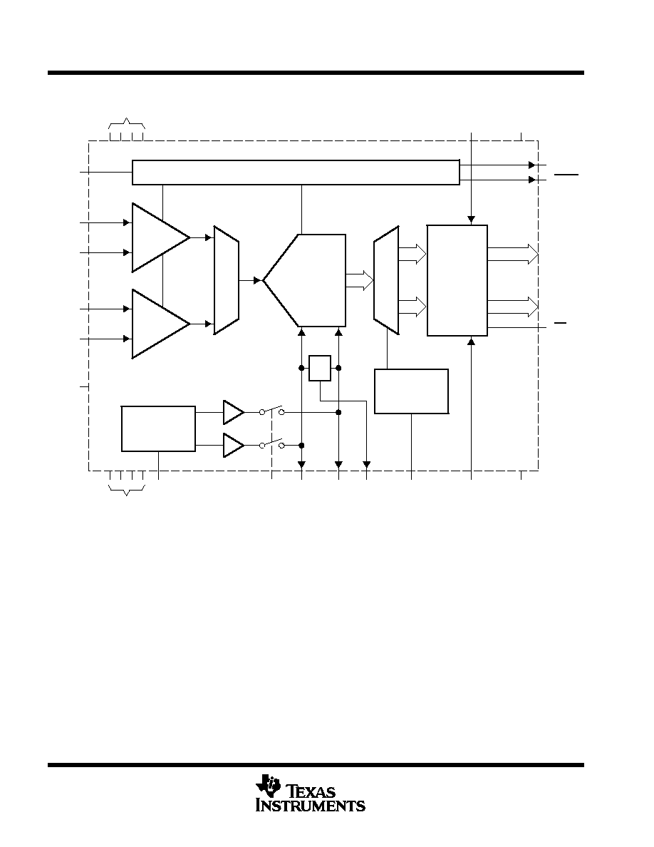
functional block diagram
MUX
Sample
& Hold
Sample
& Hold
BUS
MUX
8 BIT
ADC
3-State
Output
Buffers
Configuration
Control
Circuit
OE
DA(70)
I +
I
Q +
Q
STBY
CLK
CM
Internal
Reference
Circuit
REFT
REFB
CML
PWDN
REF
SELB
DRVSS
DVSS
DRVDD
DVDD
Timing Circuitry
AVSS
AVDD
COUT
COUT
BG
DB(70)
THS0842
DUAL-INPUT, 8-BIT, 40 MSPS LOW-POWER ANALOG-TO-DIGITAL CONVERTER
WITH SINGLE OR DUAL PARALLEL BUS OUTPUT
SLAS246 DECEMBER 1999
3
POST OFFICE BOX 655303
·
DALLAS, TEXAS 75265
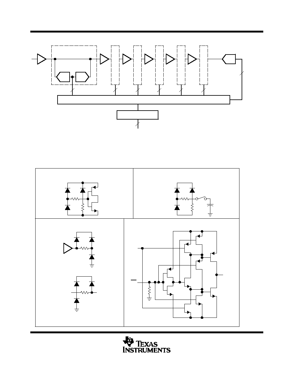
ADC pipeline block diagram
SHA
DAC
ADC
+
ADC
Correction Logic
Output Buffers
2
2
2
2
2
D0(LSB)D7(MSB)
2
2
SHA
SHA
SHA
SHA
SHA
The single-pipeline architecture uses 6 ADC/DAC stages and one final flash ADC. Each stage produces a
resolution of 2 bits. Digital correction logic generates its result using the 2-bit result from the first stage, 1 bit from
each of the 5 succeeding stages, and 1 bit from the final stage in order to arrive at an 8-bit result. The correction
logic ensures no missing codes over the full operating temperature range.
circuit diagrams of inputs and outputs
DVDD
AVDD
AVDD
0.5 pF
Internal
Reference
Generator
REFTO
or
REFBO
AVDD
REFBI
or
REFTI
OE
ALL DIGITAL INPUT CIRCUITS
AIN INPUT CIRCUIT
REFERENCE INPUT CIRCUIT
D0D7 OUTPUT CIRCUIT
DRVDD
DRVSS
D_Out
D

THS0842
DUAL-INPUT, 8-BIT, 40 MSPS LOW-POWER ANALOG-TO-DIGITAL CONVERTER
WITH SINGLE OR DUAL PARALLEL BUS OUTPUT
SLAS246 DECEMBER 1999
4
POST OFFICE BOX 655303
·
DALLAS, TEXAS 75265
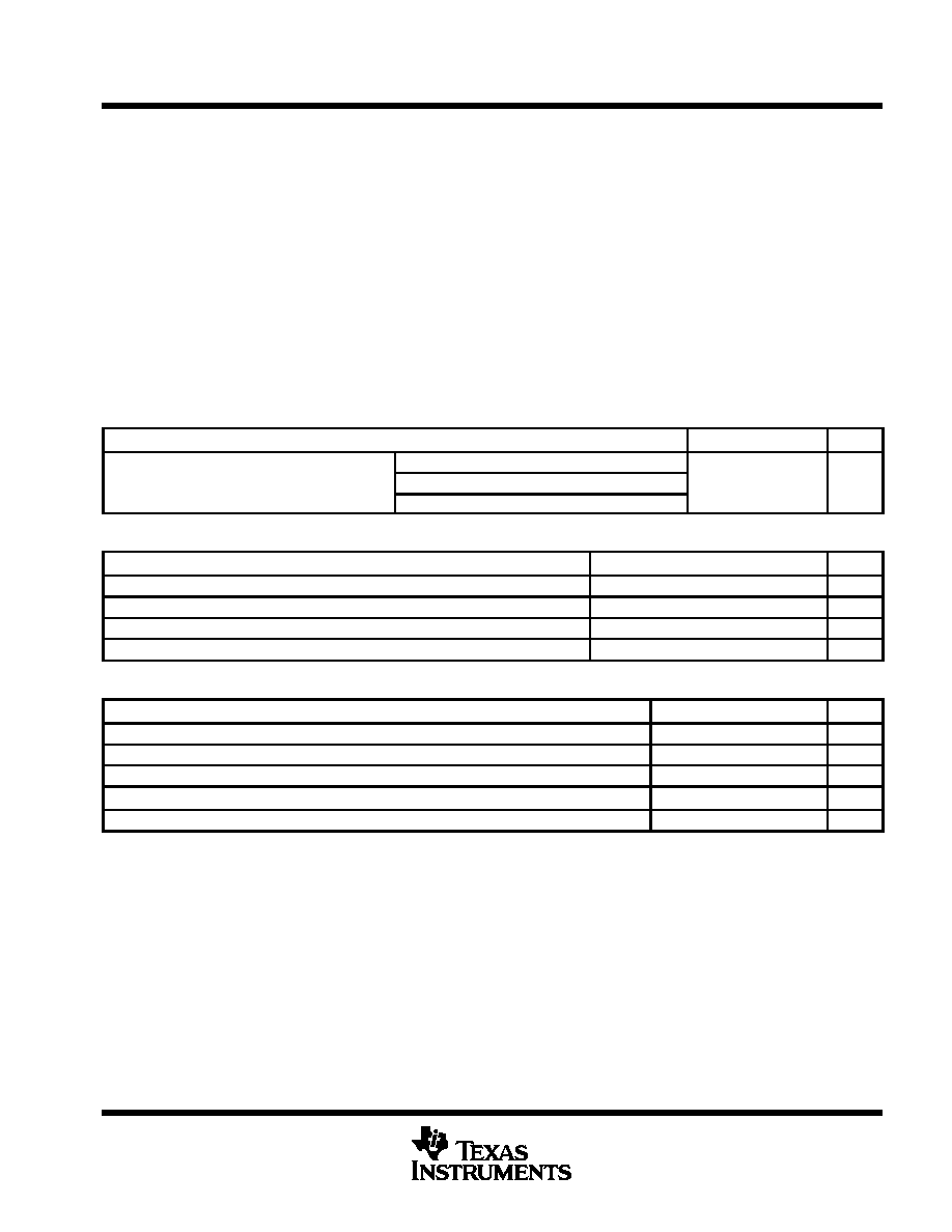
Terminal Functions
TERMINAL
I/O
DESCRIPTION
NAME
NO.
I/O
DESCRIPTION
AVDD
27, 37, 41
I
Analog supply voltage
AVSS
28, 36, 40,
46
I
Analog ground
BG
29
O
Band gap reference voltage. A 1-
µ
F capacitor with a 0.1-
µ
F capacitor in parallel should be connected
between this terminal and AVSS for external filtering.
CLK
47
I
Clock input. The input is sampled on each rising edge of CLK.
CML
32
O
Common mode level. This voltage is equal to (AVDD AVSS)/2. An external 1-
µ
F capacitor with a 0.1-
µ
F
capacitor in parallel should be connected between this terminal and AVSS.
COUT
26
O
Latch clock for the data outputs
COUT
25
O
Inverted latch clock for the data outputs
DB7 DB0
4 11
O
Data outputs. D7 is the MSB. This is the second bus. Data is output from the Q channel when dual bus
output mode is selected. Pin SELB selects the output mode.
DRVDD
1, 13
I
Supply voltage for output drivers
DRVSS
12, 24
I
Ground for digital output drivers
DA7 DA0
16 23
I
Data outputs for bus A. D7 is MSB. This is the primary bus. Data from both input channels can be output
on this bus or data from the I channel only. Pin SELB selects the output mode.
DVDD
45
I
Digital supply voltage
DVSS
43
I
Digital ground
I
39
I
Negative input for analog channel 0.
I+
38
I
Positive input for analog channel 0.
NC
2,3,14,15
No connect. Reserved for future use
OE
48
I
Output enable. A high on this terminal will disable the output bus.
PWDN_REF
33
I
Power down for internal reference voltages. A high on this terminal will disable the internal reference
circuit.
Q
35
I
Negative input for analog channel 1
Q+
34
I
Positive input for analog channel 1
REFB
30
I/O
Reference voltage bottom. The voltage at this terminal defines the bottom reference voltage for the ADC.
Sufficient filtering should be applied to this input. A 1-
µ
F capacitor with a 0.1-
µ
F capacitor in parallel should
be connected between REFB and AVSS. Additionally, a 0.1-
µ
F capacitor can be connected between REFT
and REFB.
REFT
31
I/O
Reference voltage top. The voltage at this terminal defines the top reference voltage for the ADC. Sufficient
filtering should be applied to this input. A 1-
µ
F capacitor with a 0.1-
µ
F capacitor in parallel should be
connected between REFT and AVSS. Additionally, a 0.1-
µ
F capacitor can be connected between REFT
and REFB.
SELB
44
I
Selects either single bus or data output or dual bus output data output. A low selects dual bus data output.
STBY
42
I
Standby input. A high level on this terminal will power down the device.
THS0842
DUAL-INPUT, 8-BIT, 40 MSPS LOW-POWER ANALOG-TO-DIGITAL CONVERTER
WITH SINGLE OR DUAL PARALLEL BUS OUTPUT
SLAS246 DECEMBER 1999
5
POST OFFICE BOX 655303
·
DALLAS, TEXAS 75265
absolute maximum ratings over operating free-air temperature (unless otherwise noted)
Supply voltage: AV
DD
to AGND, DV
DD
to DGND
0.5 V to 4 V
. . . . . . . . . . . . . . . . . . . . . . . . . . . . . . . . . . . . . .
Supply voltage: AV
DD
to DV
DD
, AGND to DGND
0.5 V to 0.5 V
. . . . . . . . . . . . . . . . . . . . . . . . . . . . . . . . . . . . .
Digital input voltage range to DGND
0.5 V to DV
DD
+ 0.5 V
. . . . . . . . . . . . . . . . . . . . . . . . . . . . . . . . . . . . . . . . .
Analog input voltage range to AGND
0.5 V to AV
DD
+ 0.5 V
. . . . . . . . . . . . . . . . . . . . . . . . . . . . . . . . . . . . . . . .
Digital output voltage applied from external source to DGND
0.5 V to DV
DD
+ 0.5 V
. . . . . . . . . . . . . . . . . . .
Reference voltage input range to AGND: V
(REFT)
, V
(REFB)
0.5 V to AV
DD
+ 0.5 V
. . . . . . . . . . . . . . . . . . . .
Operating free-air temperature range, T
A
: 40
°
C to 85
°
C
. . . . . . . . . . . . . . . . . . . . . . . . . . . . . . . . . . . . . . . . . .
Storage temperature range, T
stg
55
°
C to 150
°
C
. . . . . . . . . . . . . . . . . . . . . . . . . . . . . . . . . . . . . . . . . . . . . . . . . . .
Stresses beyond those listed under "absolute maximum ratings" may cause permanent damage to the device. These are stress ratings only, and
functional operation of the device at these or any other conditions beyond those indicated under "recommended operating conditions" is not
implied. Exposure to absolute-maximum-rated conditions for extended periods may affect device reliability.
recommended operating conditions over operating free-air temperature range
power supply
MIN
NOM
MAX
UNIT
AVDD
Supply voltage
DVDD
3
3.3
3.6
V
DRVDD
analog and reference inputs
MIN
NOM
MAX
UNIT
Reference input voltage (top), V(REFT)
(NOM) 0.2
AVDD 1 (NOM) + 0.2
V
Reference input voltage (bottom), V(REFB)
0.8
1
1.2
V
Reference voltage differential, V(REFT) V(REFB)
AVDD 2
V
Analog input voltage, V(IN)
V(REFB)
V(REFT)
V
digital inputs
MIN
NOM
MAX
UNIT
High-level input voltage, VIH
2.0
DVDD
V
Low-level input voltage, VIL
DGND
0.2xDVDD
V
Clock period, tc
12.5
ns
Pulse duration, clock high, tw(CLKH)
5.25
ns
Pulse duration, clock low, tw(CLKL)
5.25
ns