1
Data sheet acquired from Harris Semiconductor
SCHS181B
Features
À Buffered Inputs
À High Current Bus Driver Outputs
À Two Independent Three-State Enable Controls
À Typical Propagation Delay t
PLH
, t
PHL
= 8ns at V
CC
= 5V,
C
L
= 15pF, T
A
= 25
o
C
À Fanout (Over Temperature Range)
- Standard Outputs . . . . . . . . . . . . . . . 10 LSTTL Loads
- Bus Driver Outputs . . . . . . . . . . . . . 15 LSTTL Loads
À Wide Operating Temperature Range . . . -55
o
C to 125
o
C
À Balanced Propagation Delay and Transition Times
À Significant Power Reduction Compared to LSTTL
Logic ICs
À HC Types
- 2V to 6V Operation
- High Noise Immunity: N
IL
= 30%, N
IH
= 30% of V
CC
at V
CC
= 5V
À HCT Types
- 4.5V to 5.5V Operation
- Direct LSTTL Input Logic Compatibility,
V
IL
= 0.8V (Max), V
IH
= 2V (Min)
- CMOS Input Compatibility, I
l
1
Á
A at V
OL
, V
OH
Description
The 'HC367, 'HCT367, 'HC368, and CD74HCT368 silicon gate
CMOS three-state buffers are general purpose high-speed
non-inverting and inverting buffers. They have high drive cur-
rent outputs which enable high speed operation even when
driving large bus capacitances. These circuits possess the low
power dissipation of CMOS circuitry, yet have speeds compara-
ble to low power Schottky TTL circuits. Both circuits are capable
of driving up to 15 low power Schottky inputs.
The 'HC367 and 'HCT367 are non-inverting buffers, whereas
the 'HC368 and CD74HCT368 are inverting buffers. These
devices have two output enables, one enable (OE1) controls 4
gates and the other (OE2) controls the remaining 2 gates.
The 'HCT367 and CD74HCT368 logic families are speed, func-
tion and pin compatible with the standard LS logic family.
Ordering Information
PART NUMBER
TEMP. RANGE
(
o
C)
PACKAGE
CD54HC367F3A
-55 to 125
16 Ld CERDIP
CD74HC367E
-55 to 125
16 Ld PDIP
CD74HC367M
-55 to 125
16 Ld SOIC
CD54HCT367F3A
-55 to 125
16 Ld CERDIP
CD74HCT367E
-55 to 125
16 Ld PDIP
CD74HCT367M
-55 to 125
16 Ld SOIC
CD54HC368F
-55 to 125
16 Ld CERDIP
CD54HC368F3A
-55 to 125
16 Ld CERDIP
CD74HC368M
-55 to 125
16 Ld SOIC
CD74HCT368E
-55 to 125
16 Ld PDIP
CD74HCT368M
-55 to 125
16 Ld SOIC
NOTES:
1. When ordering, use the entire part number. Add the suffix 96 to
obtain the variant in the tape and reel.
2. Wafer or die for this part number is available which meets all
electrical specifications. Please contact your local TI sales office
or customer service for ordering information.
Pinouts
CD54HC367, CD54HCT367
(CERDIP)
CD74HC367, CD74HCT367
(PDIP, SOIC)
TOP VIEW
CD54HC368
(CERDIP)
CD74HC368, CD74HCT368
(PDIP, SOIC)
TOP VIEW
14
15
16
9
13
12
11
10
1
2
3
4
5
7
6
8
OE1
1A
1Y
2A
2Y
3A
GND
3Y
V
CC
6A
6Y
5A
5Y
4A
4Y
OE2
14
15
16
9
13
12
11
10
1
2
3
4
5
7
6
8
OE1
1A
1Y
2A
2Y
3A
GND
3Y
V
CC
6A
6Y
5A
5Y
4A
4Y
OE2
November 1997 - Revised April 2002
CAUTION: These devices are sensitive to electrostatic discharge. Users should follow proper IC Handling Procedures.
Copyright
®
2002, Texas Instruments Incorporated
CD54/74HC367, CD54/74HCT367,
CD54/74HC368, CD74HCT368
High Speed CMOS Logic Hex Buffer/Line Driver,
Three-State Non-Inverting and Inverting
[ /Title
(CD74
HC367
,
CD74
HCT36
7,
CD74
HC368
,
CD74
HCT36
8)
/Sub-
ject
(High
Speed
2
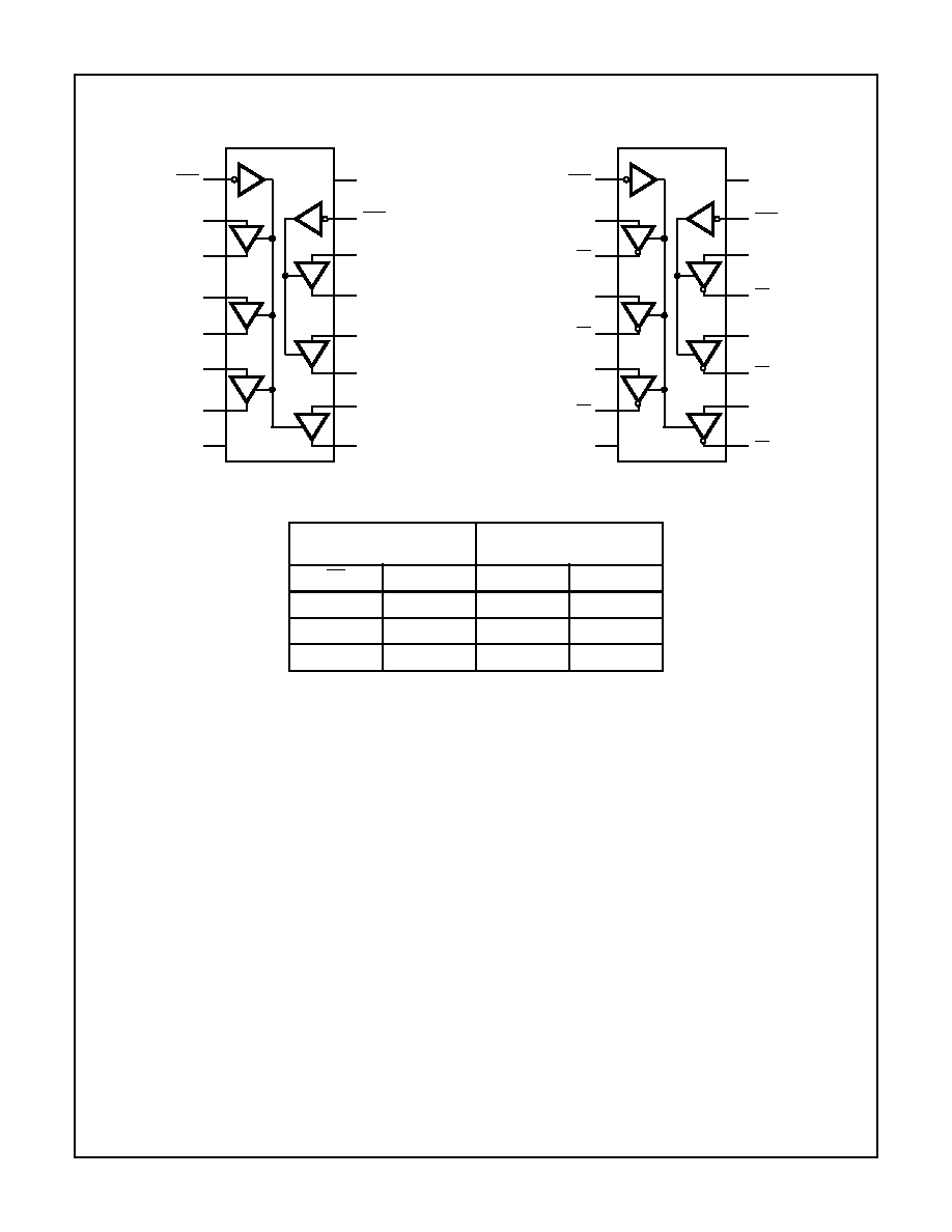
Functional Diagrams
HC367, HCT367
HC368, CD74HCT368
TRUTH TABLE
INPUTS
OUTPUTS
(Y)
OE
A
HC/HCT367
HC/HCT368
L
L
L
H
L
H
H
L
H
X
(Z)
(Z)
NOTE:
H = High Voltage Level
L = Low Voltage Level
X = Don't Care
Z = High Impedance (OFF) State
14
15
16
9
13
12
11
10
1
2
3
4
5
7
6
8
OE1
1A
1Y
2A
2Y
3A
GND
3Y
V
CC
6A
6Y
5A
5Y
4A
4Y
OE2
14
15
16
9
13
12
11
10
1
2
3
4
5
7
6
8
OE1
1A
1Y
2A
2Y
3A
GND
3Y
V
CC
6A
6Y
5A
5Y
4A
4Y
OE2
CD54/74HC367, CD54/74HCT367, CD54/74HC368, CD74HCT368
3
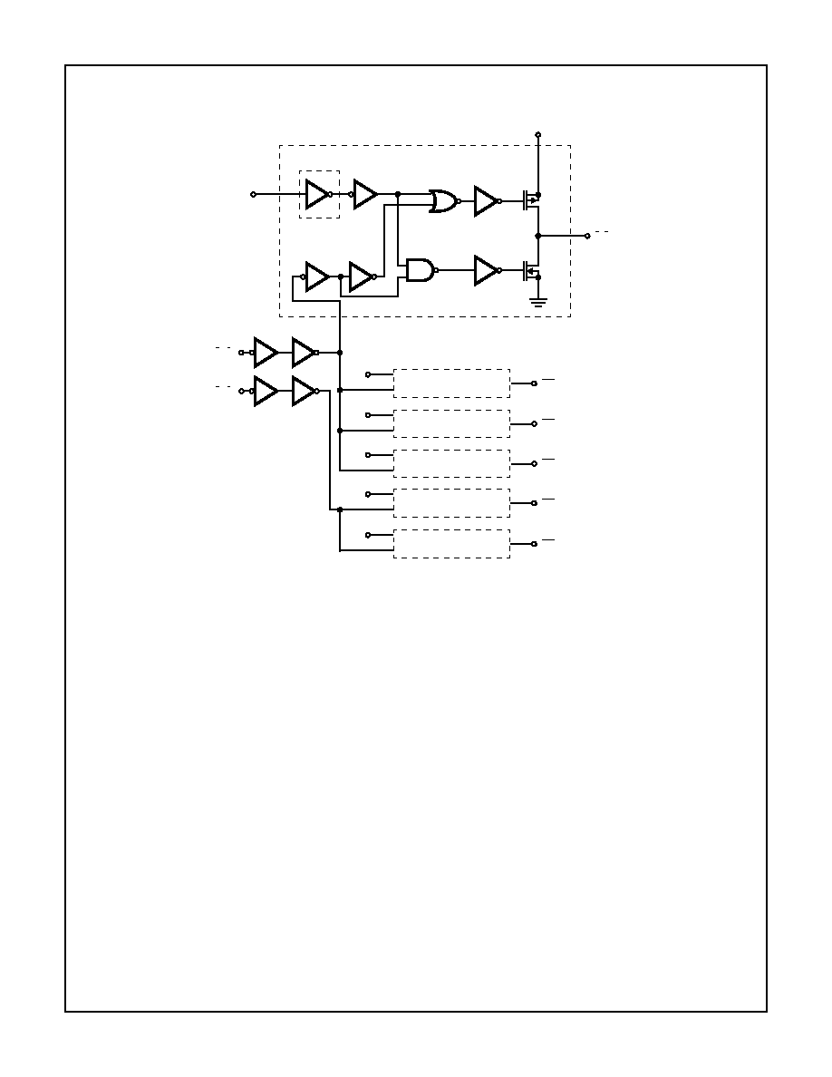
Logic Diagram
NOTE: Inverter not included in HC/HCT367.
FIGURE 1. LOGIC DIAGRAM FOR THE HC/HCT367 AND HC/HCT368 (OUTPUTS FOR HC/HCT367 ARE COMPLEMENTS OF
THOSE SHOWN, i.e., 1Y, 2Y, ETC.)
4
2A
2Y
5
6
3A
3Y
7
10
4A
4Y
9
12
5A
5Y
11
14
6A
6Y
13
OE1
1
15
OE2
ONE OF SIX IDENTICAL CIRCUITS
V
CC
3
1Y
GND
8
(NOTE)
2
1A
16
CD54/74HC367, CD54/74HCT367, CD54/74HC368, CD74HCT368

4
Absolute Maximum Ratings
Thermal Information
DC Supply Voltage, V
CC
. . . . . . . . . . . . . . . . . . . . . . . . -0.5V to 7V
DC Input Diode Current, I
IK
For V
I
< -0.5V or V
I
> V
CC
+ 0.5V
. . . . . . . . . . . . . . . . . . . . . .▒
20mA
DC Output Diode Current, I
OK
For V
O
< -0.5V or V
O
> V
CC
+ 0.5V
. . . . . . . . . . . . . . . . . . . .▒
20mA
DC Drain Current, per Output, I
O
For -0.5V < V
O
< V
CC
+ 0.5V
. . . . . . . . . . . . . . . . . . . . . . . . . .▒
35mA
DC V
CC
or Ground Current, I
CC
. . . . . . . . . . . . . . . . . . . . . . . . .▒
50mA
Operating Conditions
Temperature Range, T
A
. . . . . . . . . . . . . . . . . . . . . . -55
o
C to 125
o
C
Supply Voltage Range, V
CC
HC Types . . . . . . . . . . . . . . . . . . . . . . . . . . . . . . . . . . . . .2V to 6V
HCT Types . . . . . . . . . . . . . . . . . . . . . . . . . . . . . . . . .4.5V to 5.5V
DC Input or Output Voltage, V
I
, V
O
. . . . . . . . . . . . . . . . . 0V to V
CC
Input Rise and Fall Time
2V . . . . . . . . . . . . . . . . . . . . . . . . . . . . . . . . . . . . . . 1000ns (Max)
4.5V. . . . . . . . . . . . . . . . . . . . . . . . . . . . . . . . . . . . . . 500ns (Max)
6V . . . . . . . . . . . . . . . . . . . . . . . . . . . . . . . . . . . . . . . 400ns (Max)
Thermal Resistance (Typical, Note 3)
JA
(
o
C/W)
PDIP Package . . . . . . . . . . . . . . . . . . . . . . . . . . . . .
90
SOIC Package . . . . . . . . . . . . . . . . . . . . . . . . . . . . .
160
Maximum Junction Temperature . . . . . . . . . . . . . . . . . . . . . . . 150
o
C
Maximum Storage Temperature Range . . . . . . . . . .-65
o
C to 150
o
C
Maximum Lead Temperature (Soldering 10s) . . . . . . . . . . . . . 300
o
C
(SOIC - Lead Tips Only)
CAUTION: Stresses above those listed in "Absolute Maximum Ratings" may cause permanent damage to the device. This is a stress only rating and operation
of the device at these or any other conditions above those indicated in the operational sections of this specification is not implied.
NOTE:
3.
JA
is measured with the component mounted on an evaluation PC board in free air.
DC Electrical Specifications
PARAMETER
SYMBOL
TEST
CONDITIONS
V
CC
(V)
25
o
C
-40
o
C TO 85
o
C
-55
o
C TO 125
o
C
UNITS
V
I
(V)
I
O
(mA)
MIN
TYP
MAX
MIN
MAX
MIN
MAX
HC TYPES
High Level Input
Voltage
V
IH
-
-
2
1.5
-
-
1.5
-
1.5
-
V
4.5
3.15
-
-
3.15
-
3.15
-
V
6
4.2
-
-
4.2
-
4.2
-
V
Low Level Input
Voltage
V
IL
-
-
2
-
-
0.5
-
0.5
-
0.5
V
4.5
-
-
1.35
-
1.35
-
1.35
V
6
-
-
1.8
-
1.8
-
1.8
V
High Level Output
Voltage
CMOS Loads
V
OH
V
IH
or
V
IL
-0.02
2
1.9
-
-
1.9
-
1.9
-
V
-0.02
4.5
4.4
-
-
4.4
-
4.4
-
V
-0.02
6
5.9
-
-
5.9
-
5.9
-
V
High Level Output
Voltage
TTL Loads
-6
4.5
3.98
-
-
3.84
-
3.7
-
V
-7.8
6
5.48
-
-
5.34
-
5.2
-
V
Low Level Output
Voltage
CMOS Loads
V
OL
V
IH
or
V
IL
0.02
2
-
-
0.1
-
0.1
-
0.1
V
0.02
4.5
-
-
0.1
-
0.1
-
0.1
V
0.02
6
-
-
0.1
-
0.1
-
0.1
V
Low Level Output
Voltage
TTL Loads
6
4.5
-
-
0.26
-
0.33
-
0.4
V
7.8
6
-
-
0.26
-
0.33
-
0.4
V
Input Leakage
Current
I
I
V
CC
or
GND
-
6
-
-
▒
0.1
-
▒
1
-
▒
1
Á
A
Quiescent Device
Current
I
CC
V
CC
or
GND
0
6
-
-
8
-
80
-
160
Á
A
Three-State Leakage
Current
I
OZ
V
IL
or
V
IH
V
O
=
V
CC
or
GND
6
-
-
▒
0.5
-
▒
5.0
-
▒
10
Á
A
CD54/74HC367, CD54/74HCT367, CD54/74HC368, CD74HCT368
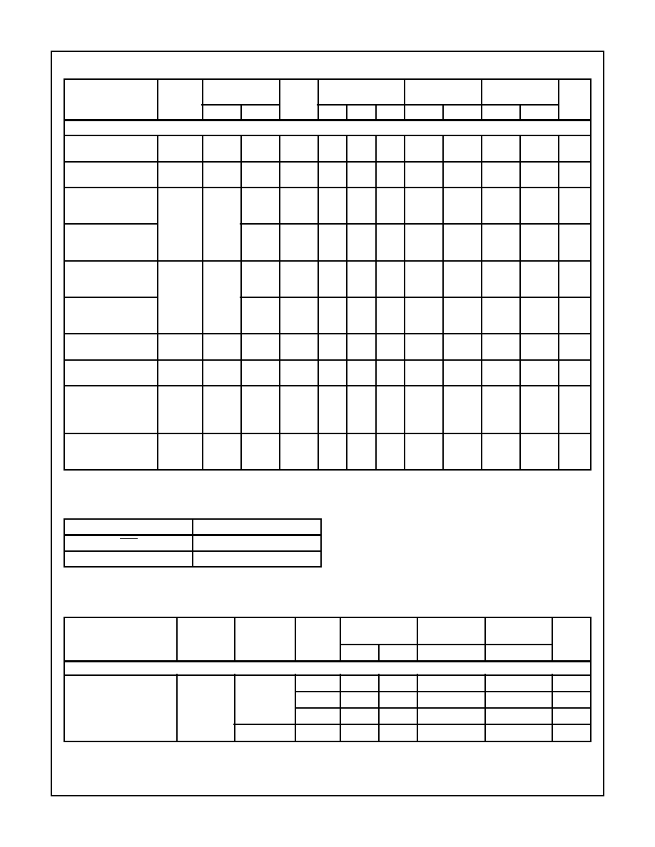
5
HCT TYPES
High Level Input
Voltage
V
IH
-
-
4.5 to
5.5
2
-
-
2
-
2
-
V
Low Level Input
Voltage
V
IL
-
-
4.5 to
5.5
-
-
0.8
-
0.8
-
0.8
V
High Level Output
Voltage
CMOS Loads
V
OH
V
IH
or
V
IL
-0.02
4.5
4.4
-
-
4.4
-
4.4
-
V
High Level Output
Voltage
TTL Loads
-4
4.5
3.98
-
-
3.84
-
3.7
-
V
Low Level Output
Voltage
CMOS Loads
V
OL
V
IH
or
V
IL
0.02
4.5
-
-
0.1
-
0.1
-
0.1
V
Low Level Output
Voltage
TTL Loads
4
4.5
-
-
0.26
-
0.33
-
0.4
V
Input Leakage
Current
I
I
V
CC
to
GND
0
5.5
-
-
▒
0.1
-
▒
1
-
▒
1
Á
A
Quiescent Device
Current
I
CC
V
CC
or
GND
0
5.5
-
-
8
-
80
-
160
Á
A
Additional Quiescent
Device Current Per
Input Pin: 1 Unit Load
(Note 4)
I
CC
V
CC
-2.1
-
4.5 to
5.5
-
100
360
-
450
-
490
Á
A
Three-State Leakage
Current
I
OZ
V
IL
or
V
IH
V
O
=
V
CC
or
GND
5.5
-
-
▒
0.5
-
▒
5.0
-
▒
10
Á
A
NOTE:
4. For dual-supply systems theoretical worst case (V
I
= 2.4V, V
CC
= 5.5V) specification is 1.8mA.
DC Electrical Specifications
(Continued)
PARAMETER
SYMBOL
TEST
CONDITIONS
V
CC
(V)
25
o
C
-40
o
C TO 85
o
C
-55
o
C TO 125
o
C
UNITS
V
I
(V)
I
O
(mA)
MIN
TYP
MAX
MIN
MAX
MIN
MAX
HCT Input Loading Table
INPUT
UNIT LOADS
OE1
0.6
All Others
0.55
NOTE: Unit Load is
I
CC
limit specified in DC Electrical
Specifications table, e.g., 360
Á
A max at 25
o
C.
Switching Specifications
Input t
r
, t
f
= 6ns
PARAMETER
SYMBOL
TEST
CONDITIONS
V
CC
(V)
25
o
C
-40
o
C TO 85
o
C
-55
o
C TO
125
o
C
UNITS
TYP
MAX
MAX
MAX
HC TYPES
Propagation Delay,
Data to Outputs
HC/HCT367
t
PLH
, t
PHL
C
L
= 50pF
2
-
105
130
160
ns
4.5
-
21
26
32
ns
6
-
18
24
27
ns
C
L
= 15pF
5
8
-
-
-
ns
CD54/74HC367, CD54/74HCT367, CD54/74HC368, CD74HCT368