bq27000
bq27010
SLUS556 Ł FEBRUARY 2003
SINGLE CELL LI ION AND LI POL BATTERY GAS GAUGE IC
FOR PORTABLE APPLICATIONS (bqJUNIOR
)
1
www.ti.com
FEATURES
D
Reports Accurate Time-to-Empty in Li-Ion
and Li-Pol Cells, No System Processor
Calculations Needed
D
Reports Cell Temperature, Voltage and
Average Current
D
High-Accuracy Coulometric Charge and
Discharge Current Integration with
Automatic Offset Cancellation
D
Requires No Offset Calibration
D
Programmable Input/Output Port
D
Internal Time-Base Eliminates External
Crystal Oscillator
D
Four Automatic Low-Power Operating Modes
Ł Active: < 100
Ą
A
Ł Sleep: < 5
Ą
A
Ł Ship: < 2
Ą
A
Ł Hibernate: < 500 nA
D
Small 8-Pin TSSOP Package
APPLICATIONS
D
PDAs
D
Smart Phones
D
MP3 Players
D
Digital Cameras
D
Internet Appliances
D
Handheld Devices
DESCRIPTION
The bqJUNIOR series are highly accurate
standalone single-cell Li-Ion and Li-Pol battery
capacity monitoring and reporting devices
targeted at space limited portable applications.
The device monitors a voltage drop across a small
current sense resistor connected in series with the
battery to determine charge and discharge activity
of the battery. Compensations for battery
temperature, selfŁdischarge, and rate of
discharge are applied to the charge counter to
provide available time-to-empty and time-to-full
information across a wide range of operating
conditions. Battery capacity is automatically
recalibrated, or learned, in the course of a
discharge cycle from full to empty. Internal
registers include available time-to-empty, cell
temperature and voltage, average current, and
other status and control registers.
The bqJUNIOR can operate directly from
single-cell Li-Ion and Li-Pol batteries and
communicates to the system over a simple
one-wire bi-directional serial interface. The
5-kbits/s HDQ bus interfaces reduces
communications overhead in the external
microcontroller.
PRODUCT PREVIEW
PRODUCT PREVIEW information concerns products in the formative or
design phase of development. Characteristic data and other
specifications are design goals. Texas Instruments reserves the right to
change or discontinue these products without notice.
Copyright
2003, Texas Instruments Incorporated
Please be aware that an important notice concerning availability, standard warranty, and use in critical applications of
Texas Instruments semiconductor products and disclaimers thereto appears at the end of this data sheet.
UDGŁ03038
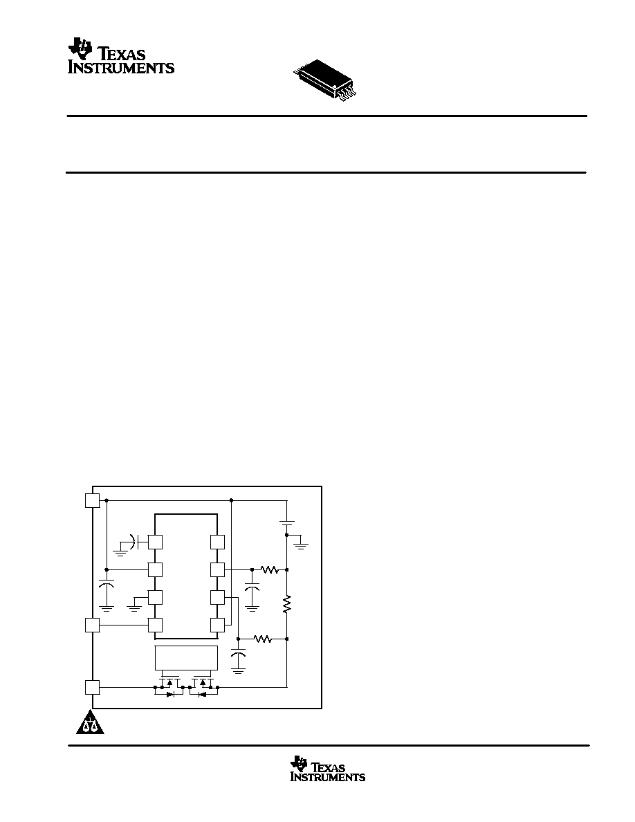
TYPICAL APPLICATION
1
2
3
4
8
7
6
5
GPIO
SRP
SRN
BAT
RBI
VCC
VSS
HDQ
bqJUNIOR
Protection
Controller
+
HDQ
PACKŁ
PACK+
Battery Pack
C4
0.1
Ą
F
C3
0.1
Ą
F
C2
0.1
Ą
F
R2
100 k
R3
100 k
C1
0.1
Ą
F
R1
0.02
Li-Ion
or
Li-Pol

bq27000
bq27010
SLUS556 Ł FEBRUARY 2003
2
www.ti.com
ABSOLUTE MAXIMUM RATINGS
over operating free-air temperature range unless otherwise noted(1) (2)
bq27000
bq27010
Supply voltage range, VCC (all with respect to VSS)
Ł0.3 V to 7.0 V
Input voltage range at SRP, SRN, RBI, and BAT (all with respect to VSS)
Ł0.3 V to VCC + 0.3 V
Inp t oltage
HDQ, GPIO (with respect to VSS)
Ł0.3 V to 7.0 V
Input voltage
GPIO (with respect to VSS) during EEPROM programming only
Ł0.3 V to 22.0 V
Output sink current at GPIO, HDQ
5 mA
Operating free-air temperature range, TA
Ł20
░
C to 70
░
C
Storage temperature range, Tstg
Ł65
░
C to 150
░
C
Junction temperature range, TJ
Ł40
░
C to 125
░
C
Lead temperature 1,6 mm (1/16 inch) from case for 10 seconds
300
░
C
(1) Stresses beyond those listed under "absolute maximum ratings" may cause permanent damage to the device. These are stress ratings only,
and functional operation of the device at these or any other conditions beyond those indicated under "recommended operating conditions" is
not implied. Exposure to Absolute Maximum Rated conditions for extended periods may affect device reliability
RECOMMENDED OPERATING CONDITIONS
MIN
NOM
MAX
UNIT
Supply voltage, VCC
2.6
4.5
V
Operating free-air temperature, TJ
Ł20
70
░
C
ELECTRICAL CHARACTERISTICS
TJ = Ł20
░
C to 70
░
C, TJ = TA, 2.6 V
VCC
4.5 V (unless otherwise noted)
PARAMETER
TEST CONDITIONS
MIN
TYP
MAX
UNIT
INPUT CURRENTS
ICC(VCC) Input current, VCC
VCC > VCC(min)
100
ICC(SLP) Sleep current
5
Ą
A
ICC(SHP) Ship current
2
Ą
A
ICC(POR) Hibernate current
0 V < VCC < V(POR)
500
nA
EEPROM programming current
VPROGRAM = 21 V
15
mA
RBI current
RBI pin only,
VCC < V(POR)
20
nA
V(POR)
POR threshold
2.0
2.5
V
RBI data retention voltage
1.2
V
Input impedance on BAT pin
10
M
Input impedance on SRR, SRN pins
10
M
VOLTAGE MEASUREMENT
Measurement range
VCC = VI(BAT)
2.6
4.5
V
Reported voltage resolution
2.7
mV
Reported accuracy
Ł25
25
mV
Voltage update time
2
s
VOLTAGE MEASUREMENT
Reported temperature resolution
0.25
░
K
Reported temperature accuracy
Ł3
3
░
K
Temperature update time
2
s
PRODUCT PREVIEW
bq27000
bq27010
SLUS556 Ł FEBRUARY 2003
3
www.ti.com
ELECTRICAL CHARACTERISTICS (continued)
TJ = Ł20
░
C to 70
░
C, TJ = TA, 2.6 V
VCC
4.5 V (unless otherwise noted)
PARAMETER
TEST CONDITIONS
MIN
TYP
MAX
UNIT
EEPROM PROGRAMMING VOLTAGE
tRISE
Programming voltage rise time
0.5
1.5
Programming voltage high time
10
100
ms
tFALL
Programming voltage fall time
0.5
1.5
ms
Programming voltage
Applied to GPIO pin
20
22
V
IO PORT (GPIO) AND SERIAL INTERFACE (HDQ)
V
High le el inp t oltage
VCC < 4.2 V
1.7
VIH
High-level input voltage
VCC > 4.2 V
1.9
V
VIL
Low-level input voltage
0.7
V
IOL
Low-level output current
VOL > 0.4 V
1
mA
STANDARD SERIAL COMMUNICATION (HDQ) TIMING(1)
T(B)
Break timing
190
T(BR)
Break recovery time
40
T(CYCH) Host bit window timing
190
T(HW1)
Host sends 1 time
5
50
T(HW0)
Host sends 0 time
100
145
Ą
s
T(RSPS)
bq27000 to host response time
190
320
Ą
s
T(CYCB)
bq27000 bit window timing
190
250
T(DW1)
bq27000 sends 1 time
32
50
T(DW0)
bq27000 sends 0 time
80
145
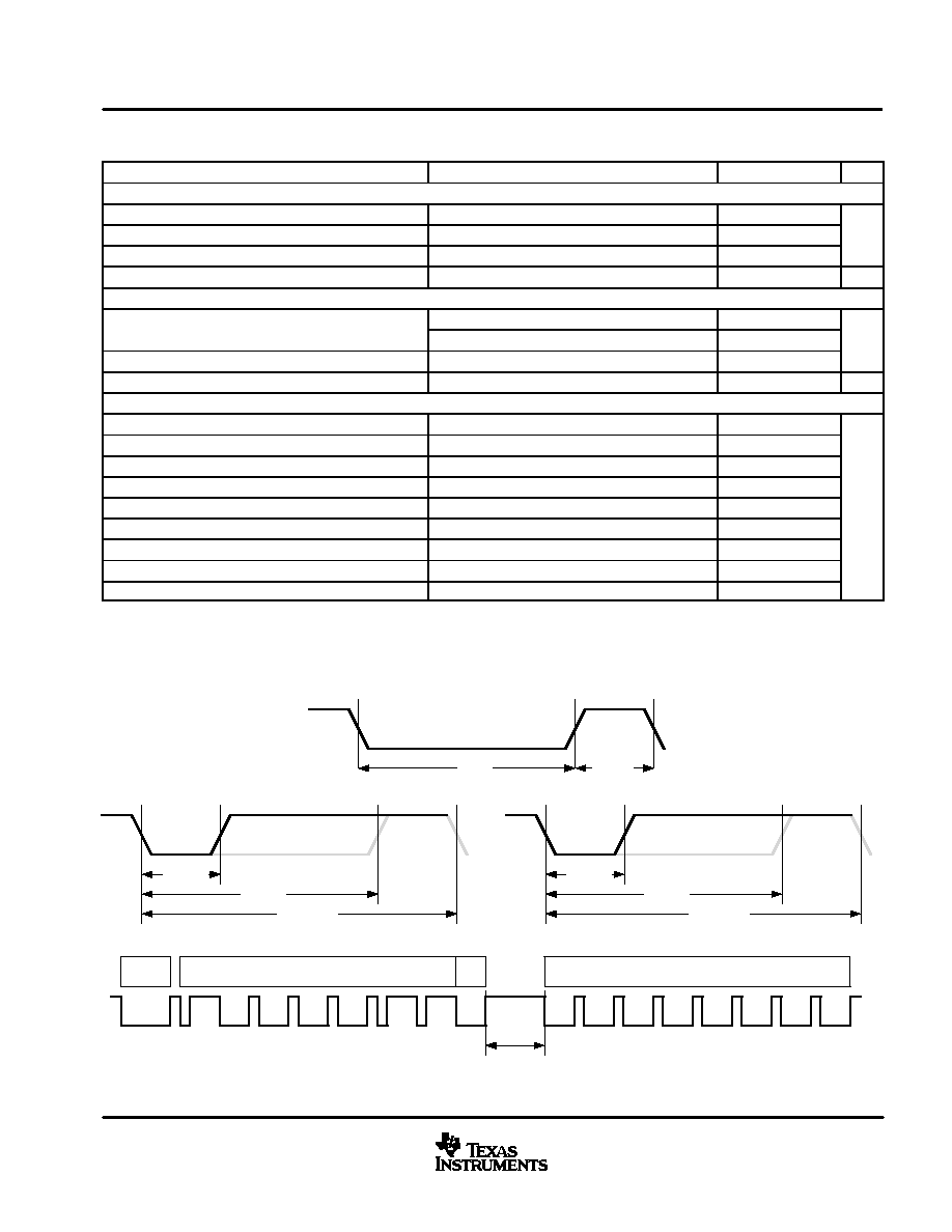
(1) See Figure 1.
The following timing diagrams describe break and break recovery timing (a), host transmitted bit timing (b),
bqJUNIOR transmitted bit timing (c), and bqJUNIOR to host response timing (d).
UDGŁ03039
(a)
(b)
(c)
(d)
Break
7ŁBit Address
R/W
8ŁBit Data
t(B)
t(BR)
1Łbit
t(HW1)
t(DW1)
t(HW0)
t(DW1)
t(CYCH)
t(CYCD)
t(RSPS)
Figure 1. HDQ Bit Timing Diagrams
PRODUCT PREVIEW

bq27000
bq27010
SLUS556 Ł FEBRUARY 2003
4
www.ti.com
PIN ASSIGNMENTS
TERMINAL
I/O
DESCRIPTION
NAME
NO.
I/O
DESCRIPTION
BAT
5
I
Battery voltage sense input
GPIO
8
I/O
General-purpose input/output port
HDQ
4
I/O
Single-wire HDQ serial interface
RBI
1
I
Register back-up input
SRN
6
I
Current sense input (positive)
SRP
7
I
Current sense input (negative)
VCC
2
I
VCC supply input
VSS
3
I
Ground input
1
2
3
4
8
7
6
5
RBI
VCC
VSS
HDQ
GPIO
SRP
SRN
BAT
PW PACKAGE
(TOP VIEW)
AVAILABLE OPTIONS
TA
ADDITIONAL FUNCTIONS
PACKAGED
DEVICES
MARKINGS
Ł20
░
C to 70
░
C
TTECP, AP, SAE, MLTTE, MLI,
STTE, SI, ARTTE, and AR
bq27000PW
20 C to 70 C
bq27010PW
The PW package is available taped and reeled. Add R suffix to device type (e.g. bq27000PWR)
to order quantities of 2,000 devices per reel.
PRODUCT PREVIEW
bq27000
bq27010
SLUS556 Ł FEBRUARY 2003
5
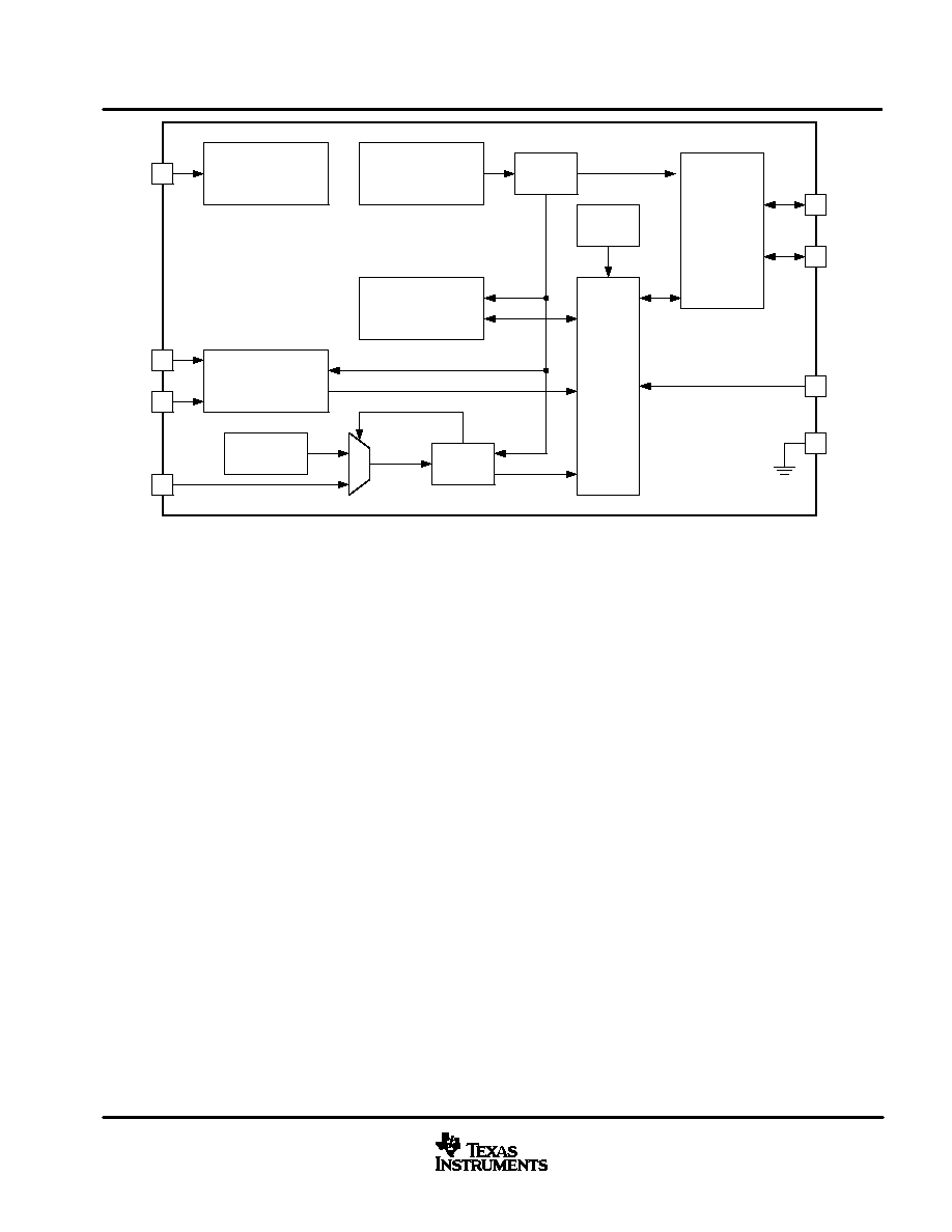
www.ti.com
Temperature
Compensated
Precision Oscillator
Clock
Generator
EEPROM
RAM
SCPU
System I/O
and Control
Temperature
Sensor
ADC
2
VCC
7
SRP
6
SRN
5
BAT
4
HDQ
8
GPIO
1
RBI
3
VSS
Autocalibration and
Autocompensating
VFC
UDGŁ03040
Bandgap
Reference and
Bias
Figure 2. Functional Block Diagram
PRODUCT PREVIEW