www.ti.com
FEATURES
DESCRIPTION
136
-128
-144
-160
0.4
0.8
1.2
1.6
2.0
2.4
2.8
170
153
119
102
85
68
51
34
17
0
0.4
0.8
1.2
1.6
2.0
2.4
2.8
3.2
T
A
= 25
°
C
Process = Nominal
I
OL
- Output Current - mA
V
CC
= 3.3 V
V
CC
= 2.5 V
V
CC
= 1.8 V
- Output V
oltage - V
OL
V
T
A
= 25
°
C
Process = Nominal
I
OH
- Output Current - mA
V
CC
= 3.3 V
V
CC
= 2.5 V
V
CC
= 1.8 V
- Output V
oltage - V
OH
V
-80
-96
-112
-32
-48
-64
0
-16
SN74AVC16646
16-BIT BUS TRANSCEIVER AND REGISTER
WITH 3-STATE OUTPUTS
SCES181F DECEMBER 1998 REVISED JUNE 2005
·
Overvoltage-Tolerant Inputs/Outputs Allow
Mixed-Voltage-Mode Data Communications
·
Member of the Texas Instruments WidebusTM
Family
·
I
off
Supports Partial-Power-Down Mode
Operation
·
EPICTM (Enhanced-Performance Implanted
CMOS) Submicron Process
·
Latch-Up Performance Exceeds 100 mA Per
JESD 78, Class II
·
DOCTM (Dynamic Output Control) Circuit
Dynamically Changes Output Impedance,
·
Package Options Include Plastic Thin Shrink
Resulting in Noise Reduction Without Speed
Small-Outline (DGG) and Thin Very
Degradation
Small-Outline (DGV) Packages
·
Dynamic Drive Capability Is Equivalent to
Standard Outputs With I
OH
and I
OL
of
±
24 mA
at 2.5-V V
CC
A Dynamic Output Control (DOCTM) circuit is implemented, which, during the transition, initially lowers the output
impedance to effectively drive the load and, subsequently, raises the impedance to reduce noise.
Figure 1
shows
typical V
OL
vs I
OL
and V
OH
vs I
OH
curves to illustrate the output impedance and drive capability of the circuit. At
the beginning of the signal transition, the DOC circuit provides a maximum dynamic drive that is equivalent to a
high-drive standard-output device. For more information, refer to the TI application reports, AVC Logic Family
Technology and Applications, literature number SCEA006, and Dynamic Output Control (DOCTM) Circuitry
Technology and Applications, literature number SCEA009.
Figure 1. Output Voltage vs Output Current
This 16-bit bus transceiver and register is operational at 1.2-V to 3.6-V V
CC
, but is designed specifically for
1.65-V to 3.6-V V
CC
operation.
The SN74AVC16646 can be used as two 8-bit transceivers or one 16-bit transceiver. Data on the A or B bus is
clocked into the registers on the low-to-high transition of the appropriate clock (CLKAB or CLKBA) input.
Figure 2
illustrates the four fundamental bus-management functions that can be performed with the SN74AVC16646.
Output-enable (OE) and direction-control (DIR) inputs are provided to control the transceiver functions. In the
transceiver mode, data present at the high-impedance port may be stored in either register or in both. The
select-control (SAB and SBA) inputs can multiplex stored and real-time (transparent mode) data.
Please be aware that an important notice concerning availability, standard warranty, and use in critical applications of Texas
Instruments semiconductor products and disclaimers thereto appears at the end of this data sheet.
Widebus, EPIC, DOC are trademarks of Texas Instruments.
PRODUCTION DATA information is current as of publication date.
Copyright © 19982005, Texas Instruments Incorporated
Products conform to specifications per the terms of the Texas
Instruments standard warranty. Production processing does not
necessarily include testing of all parameters.

www.ti.com
DESCRIPTION (CONTINUED)
TERMINAL ASSIGNMENTS
DGG OR DGV PACKAGE
(TOP VIEW)
1
2
3
4
5
6
7
8
9
10
11
12
13
14
15
16
17
18
19
20
21
22
23
24
25
26
27
28
56
55
54
53
52
51
50
49
48
47
46
45
44
43
42
41
40
39
38
37
36
35
34
33
32
31
30
29
1DIR
1CLKAB
1SAB
GND
1A1
1A2
V
CC
1A3
1A4
1A5
GND
1A6
1A7
1A8
2A1
2A2
2A3
GND
2A4
2A5
2A6
V
CC
2A7
2A8
GND
2SAB
2CLKAB
2DIR
1OE
1CLKBA
1SBA
GND
1B1
1B2
V
CC
1B3
1B4
1B5
GND
1B6
1B7
1B8
2B1
2B2
2B3
GND
2B4
2B5
2B6
V
CC
2B7
2B8
GND
2SBA
2CLKBA
2OE
SN74AVC16646
16-BIT BUS TRANSCEIVER AND REGISTER
WITH 3-STATE OUTPUTS
SCES181F DECEMBER 1998 REVISED JUNE 2005
The circuitry used for select control eliminates the typical decoding glitch that occurs in a multiplexer during the
transition between stored and real-time data. DIR determines which bus receives data when OE is low. In the
isolation mode (OE high), A data may be stored in one register and/or B data may be stored in the other register.
When an output function is disabled, the input function still is enabled and may be used to store and transmit
data. Only one of the two buses, A or B, can be driven at a time.
To ensure the high-impedance state during power up or power down, OE should be tied to V
CC
through a pullup
resistor; the minimum value of the resistor is determined by the current-sinking capability of the driver.
This device is fully specified for partial-power-down applications using I
off
. The I
off
circuitry disables the outputs,
preventing damaging current backflow through the device when it is powered down.
The SN74AVC16646 is characterized for operation from 40°C to 85°C.
2

www.ti.com
SN74AVC16646
16-BIT BUS TRANSCEIVER AND REGISTER
WITH 3-STATE OUTPUTS
SCES181F DECEMBER 1998 REVISED JUNE 2005
FUNCTION TABLE
(EACH 8-BIT TRANSCEIVER/REGISTER)
INPUTS
DATA I/Os
OPERATION OR FUNCTION
OE
DIR
CLKAB
CLKBA
SAB
SBA
A1-A8
B1-B8
X
X
X
X
X
Input
Unspecified
(1)
Store A, B unspecified
(1)
X
X
X
X
X
Unspecified
(1)
Input
Store B, A unspecified
(1)
H
X
X
X
Input
Input
Store A and B data
H
X
H or L
H or L
X
X
Input disabled
Input disabled
Isolation, hold storage
L
L
X
X
X
L
Output
Input
Real-time B data to A bus
L
L
X
H or L
X
H
Output
Input
Stored B data to A bus
L
H
X
X
L
X
Input
Output
Real-time A data to B bus
L
H
H or L
X
H
X
Input
Output
Stored A data to B bus
(1)
The data-output functions may be enabled or disabled by various signals at OE and DIR. Data-input functions always are enabled; i.e.,
data at the bus terminals is stored on every low-to-high transition of the clock inputs.
3

www.ti.com
L
DIR
L
CLKAB
X
CLKBA
X
SAB
X
SBA
L
L
DIR
H
CLKAB
X
CLKBA
X
SAB
L
SBA
X
X
DIR
X
CLKAB CLKBA
X
SAB
X
SBA
X
L
DIR
L
CLKAB
X
CLKBA
H or L
SAB
X
SBA
H
X
H
X
X
X
X
X
X
X
L
H
H or L
X
H
X
BUS B
BUS
A
BUS B
BUS
A
BUS B
BUS
A
BUS B
BUS
A
OE
OE
OE
OE
REAL-TIME TRANSFER
BUS B TO BUS A
REAL-TIME TRANSFER
BUS A TO BUS B
STORAGE FROM
A, B, OR A AND B
TRANSFER STORED DATA
TO A AND/OR B
SN74AVC16646
16-BIT BUS TRANSCEIVER AND REGISTER
WITH 3-STATE OUTPUTS
SCES181F DECEMBER 1998 REVISED JUNE 2005
Figure 2. Bus-Management Functions
4

www.ti.com
1A2
6
1A3
8
1A4
9
1A5
10
1A6
12
1A7
13
1A8
14
2A2
16
2A3
17
2A4
19
2A5
20
2A6
21
2A7
23
2A8
24
5
1A1
1B6
45
1B7
44
1B8
43
1B2
51
1B3
49
1B4
48
1B5
47
1B1
52
4D
1
2
G12
31
2SBA
30
2CLKBA
10 EN8 [BA]
28
2DIR
G10
29
2B6
36
2B7
34
2B8
33
2B2
41
2B3
40
2B4
38
2B5
37
2OE
10 EN9 [AB]
1
1
5
5
1
1
7
7
15
2A1
8
9
1
1
12
12
1
1
14
14
13D
2B1
42
11D
C11
G14
26
2SAB
27
2CLKAB
C13
G5
54
1SBA
55
1CLKBA
3 EN1 [BA]
1
1DIR
G3
56
1OE
3 EN2 [AB]
C4
G7
3
1SAB
2
1CLKAB
C6
6D
(1) This symbol is in accordance with ANSI/IEEE Std 91-1984 and IEC Publication 617-12.
SN74AVC16646
16-BIT BUS TRANSCEIVER AND REGISTER
WITH 3-STATE OUTPUTS
SCES181F DECEMBER 1998 REVISED JUNE 2005
LOGIC SYMBOL
(1)
5

www.ti.com
LOGIC DIAGRAM (POSITIVE LOGIC)
1A1
1B1
1D
C1
1D
C1
One of Eight Channels
52
5
3
2
54
55
56
1
1SAB
1CLKAB
1SBA
1CLKBA
1DIR
1OE
To Seven Other Channels
2A1
2B1
1D
C1
1D
C1
42
15
26
27
31
30
29
28
2SAB
2CLKAB
2SBA
2CLKBA
2DIR
2OE
To Seven Other Channels
One of Eight Channels
SN74AVC16646
16-BIT BUS TRANSCEIVER AND REGISTER
WITH 3-STATE OUTPUTS
SCES181F DECEMBER 1998 REVISED JUNE 2005
6
www.ti.com
Absolute Maximum Ratings
(1)
SN74AVC16646
16-BIT BUS TRANSCEIVER AND REGISTER
WITH 3-STATE OUTPUTS
SCES181F DECEMBER 1998 REVISED JUNE 2005
over operating free-air temperature range (unless otherwise noted)
MIN
MAX
UNIT
V
CC
Supply voltage range
0.5
4.6
V
V
I
Input voltage range
(2)
0.5
4.6
V
Voltage range applied to any input/output
V
O
0.5
4.6
V
when the output is in the high-impedance or power-off state
(2)
V
O
Voltage range applied to any input/output when the output is in the high or low state
(2) (3)
0.5
V
CC
+ 0.5
V
I
IK
Input clamp current
V
I
< 0
50
mA
I
OK
Output clamp current
V
O
< 0
50
mA
I
O
Continuous output current
±50
mA
Continuous current through each V
CC
or GND
±100
mA
DGG package
64
JA
Package thermal impedance
(4)
°C/W
DGV package
48
T
stg
Storage temperature range
65
150
°C
(1)
Stresses beyond those listed under "absolute maximum ratings" may cause permanent damage to the device. These are stress ratings
only, and functional operation of the device at these or any other conditions beyond those indicated under "recommended operating
conditions" is not implied. Exposure to absolute-maximum-rated conditions for extended periods may affect device reliability.
(2)
The input and output negative-voltage ratings may be exceeded if the input and output current ratings are observed.
(3)
The output positive-voltage rating may be exceeded up to 4.6 V maximum if the output current rating is observed.
(4)
The package thermal impedance is calculated in accordance with JESD 51.
7

www.ti.com
Recommended Operating Conditions
(1)
SN74AVC16646
16-BIT BUS TRANSCEIVER AND REGISTER
WITH 3-STATE OUTPUTS
SCES181F DECEMBER 1998 REVISED JUNE 2005
MIN
MAX
UNIT
V
CC
Supply voltage
Operating
1.2
3.6
V
V
CC
= 1.2 V
V
CC
V
CC
= 1.4 V to 1.6 V
0.65 × V
CC
V
IH
High-level input voltage
V
CC
= 1.65 V to 1.95 V
0.65 × V
CC
V
V
CC
= 2.3 V to 2.7 V
1.7
V
CC
= 3 V to 3.6 V
2
V
CC
= 1.2 V
GND
V
CC
= 1.4 V to 1.6 V
0.35 × V
CC
V
IL
Low-level input voltage
V
CC
= 1.65 V to 1.95 V
0.35 × V
CC
V
V
CC
= 2.3 V to 2.7 V
0.7
V
CC
= 3 V to 3.6 V
0.8
V
I
Input voltage
0
3.6
V
Active state
0
V
CC
V
O
Output voltage
V
3-state
0
3.6
V
CC
= 1.4 V to 1.6 V
2
V
CC
= 1.65 V to 1.95 V
4
I
OHS
Static high-level output current
(2)
mA
V
CC
= 2.3 V to 2.7 V
8
V
CC
= 3 V to 3.6 V
12
V
CC
= 1.4 V to 1.6 V
2
V
CC
= 1.65 V to 1.95 V
4
I
OLS
Static low-level output current
(2)
mA
V
CC
= 2.3 V to 2.7 V
8
V
CC
= 3 V to 3.6 V
12
t/
v
Input transition rise or fall rate
V
CC
= 1.4 V to 3.6 V
5
ns/V
T
A
Operating free-air temperature
40
85
°C
(1)
All unused inputs of the device must be held at V
CC
or GND to ensure proper device operation. Refer to the TI application report,
Implications of Slow or Floating CMOS Inputs, literature number SCBA004.
(2)
Dynamic drive capability is equivalent to standard outputs with I
OH
and I
OL
of ±24 mA at 3.3-V V
CC
. See Figure 1 for V
OL
vs I
OL
and V
OH
vs I
OH
characteristics. Refer to the TI application reports, AVC Logic Family Technology and Applications, literature number SCEA006,
and Dynamic Output Control (DOCTM) Circuitry Technology and Applications, literature number SCEA009.
8

www.ti.com
Electrical Characteristics
Timing Requirements
SN74AVC16646
16-BIT BUS TRANSCEIVER AND REGISTER
WITH 3-STATE OUTPUTS
SCES181F DECEMBER 1998 REVISED JUNE 2005
over recommended operating free-air temperature range (unless otherwise noted)
PARAMETER
TEST CONDITIONS
V
CC
MIN
TYP
(1)
MAX
UNIT
I
OHS
= 100
µ
A
1.2 V to 3.6 V
V
CC
0.2
I
OHS
= 2 mA,
V
IH
= 0.91 V
1.4 V
1.05
V
OH
I
OHS
= 4 mA,
V
IH
= 1.07 V
1.65 V
1.2
V
I
OHS
= 8 mA,
V
IH
= 1.7 V
2.3 V
1.75
I
OHS
= 12 mA,
V
IH
= 2 V
3 V
2.3
I
OLS
= 100
µ
A
1.2 V to 3.6 V
0.2
I
OLS
= 2 mA,
V
IL
= 0.49 V
1.4 V
0.4
V
OL
I
OLS
= 4 mA,
V
IL
= 0.57 V
1.65 V
0.45
V
I
OLS
= 8 mA,
V
IL
= 0.7 V
2.3 V
0.55
I
OLS
= 12 mA,
V
IL
= 0.8 V
3 V
0.7
I
I
Control inputs
V
I
= V
CC
or GND
3.6 V
±2.5
µ
A
I
off
V
I
or V
O
= 3.6 V
0
±10
µ
A
I
OZ
(2)
V
O
= V
CC
or GND,
V
I
= V
CC
3.6 V
±12.5
µ
A
I
CC
V
I
= V
CC
or GND,
I
O
= 0
3.6 V
40
µ
A
2.5 V
3
CLK inputs
3.3 V
3
C
i
V
I
= V
CC
or GND
pF
2.5 V
3.5
Control inputs
3.3 V
3.5
2.5 V
8
C
io
A or B ports
V
O
= V
CC
or GND
pF
3.3 V
8
(1)
Typical values are measured at T
A
= 25°C.
(2)
For I/O ports, the parameter I
OZ
includes the input leakage current.
over recommended operating free-air temperature range (unless otherwise noted) (see
Figure 3
through
Figure 6
)
V
CC
= 1.5 V
V
CC
= 1.8 V
V
CC
= 2.5 V
V
CC
= 3.3 V
V
CC
= 1.2 V
± 0.1 V
± 0.15 V
± 0.2 V
± 0.3 V
UNIT
MIN
MAX
MIN
MAX
MIN
MAX
MIN
MAX
MIN
MAX
f
clock
Clock frequency
150
250
350
MHz
Pulse
CLKAB or CLKBA
t
w
3.3
2
1.4
ns
duration
high or low
A before CLKAB
or
t
su
Setup time
2.1
1.6
1.2
0.9
0.8
ns
B before CLKBA
A after CLKAB
or
t
h
Hold time
1.3
1
0.8
0.6
0.6
ns
B after CLKBA
9

www.ti.com
Switching Characteristics
Operating Characteristics
SN74AVC16646
16-BIT BUS TRANSCEIVER AND REGISTER
WITH 3-STATE OUTPUTS
SCES181F DECEMBER 1998 REVISED JUNE 2005
over recommended operating free-air temperature range (unless otherwise noted) (see
Figure 3
through
Figure 6
)
V
CC
= 1.5 V
V
CC
= 1.8 V
V
CC
= 2.5 V
V
CC
= 3.3 V
V
CC
= 1.2 V
FROM
TO
± 0.1 V
± 0.15 V
± 0.2 V
± 0.3 V
PARAMETER
UNIT
(INPUT)
(OUTPUT)
TYP
MIN
MAX
MIN
MAX
MIN
MAX
MIN
MAX
f
max
150
250
350
MHz
A or B
B or A
4.2
1.6
4.8
1.5
4.3
1.2
3.1
0.9
2.6
CLKAB or
t
pd
5.9
2.2
7.4
1.9
6.1
1.3
4
1
3.3
ns
CLKBA
A or B
SAB or SBA
8.2
2.6
10
2.4
6.3
1.8
5.1
1.5
4
t
en
OE
A or B
6.5
2.2
8
1.9
7
1.4
4.6
1.1
4
ns
t
dis
OE
A or B
6.7
2.6
8
2.6
7.2
1.4
4.3
1.4
4.2
ns
t
en
DIR
A or B
6.9
2.2
8.7
1.9
7.4
1.4
5
1.1
4.3
ns
t
dis
DIR
A or B
7.5
2.6
8.7
2.6
7.6
1.4
4.5
1.4
4.3
ns
T
A
= 25°C
V
CC
= 1.8 V
V
CC
= 2.5 V
V
CC
= 3.3 V
PARAMETER
TEST CONDITIONS
UNIT
TYP
TYP
TYP
Outputs enabled
62
73
120
C
pd
Power dissipation capacitance
C
L
= 0,
f = 10 MHz
pF
Outputs disabled
25
29
34
10
www.ti.com
PARAMETER MEASUREMENT INFORMATION
V
CC
/2
V
CC
/2
V
CC
/2
V
CC
/2
V
CC
/2
V
CC
/2
V
CC
/2
V
CC
/2
V
OH
V
OL
t
h
t
su
From Output
Under Test
C
L
= 15 pF
(see Note A)
LOAD CIRCUIT
S1
Open
GND
2 k
2 k
Output
Control
(low-level
enabling)
Output
Waveform 1
S1 at 2
×
V
CC
(see Note B)
Output
Waveform 2
S1 at GND
(see Note B)
t
PZL
t
PZH
t
PLZ
t
PHZ
0 V
V
OL
+ 0.1 V
V
OH
- 0.1 V
0 V
V
CC
0 V
0 V
t
w
V
CC
V
CC
VOLTAGE WAVEFORMS
SETUP AND HOLD TIMES
VOLTAGE WAVEFORMS
PULSE DURATION
VOLTAGE WAVEFORMS
ENABLE AND DISABLE TIMES
Timing
Input
Data
Input
Input
t
pd
t
PLZ
/t
PZL
t
PHZ
/t
PZH
Open
2
×
V
CC
GND
TEST
S1
NOTES: A. C
L
includes probe and jig capacitance.
B. Waveform 1 is for an output with internal conditions such that the output is low, except when disabled by the output control.
Waveform 2 is for an output with internal conditions such that the output is high, except when disabled by the output control.
C. All input pulses are supplied by generators having the following characteristics: PRR
10 MHz, Z
O
= 50
, t
r
2 ns, t
f
2 ns.
D. The outputs are measured one at a time, with one transition per measurement.
E. t
PLZ
and t
PHZ
are the same as t
dis
.
F. t
PZL
and t
PZH
are the same as t
en
.
G. t
PLH
and t
PHL
are the same as t
pd
.
0 V
V
CC
V
CC
/2
t
PHL
V
CC
/2
V
CC
/2
V
CC
0 V
V
OH
V
OL
Input
Output
VOLTAGE WAVEFORMS
PROPAGATION DELAY TIMES
V
CC
/2
V
CC
/2
t
PLH
2
×
V
CC
V
CC
SN74AVC16646
16-BIT BUS TRANSCEIVER AND REGISTER
WITH 3-STATE OUTPUTS
SCES181F DECEMBER 1998 REVISED JUNE 2005
V
CC
= 1.2 V AND 1.5 V ± 0.1 V
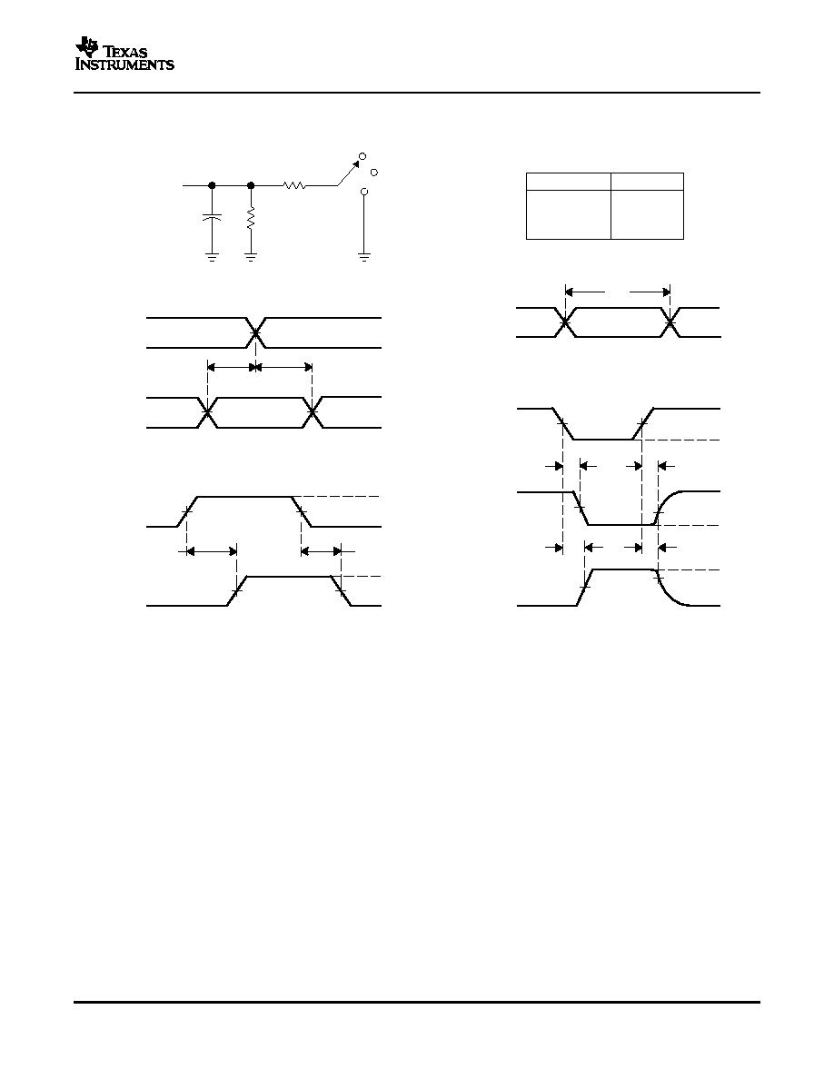
Figure 3. Load Circuit and Voltage Waveforms
11
www.ti.com
PARAMETER MEASUREMENT INFORMATION
V
CC
/2
V
CC
/2
V
CC
/2
V
CC
/2
V
CC
/2
V
CC
/2
V
CC
/2
V
CC
/2
V
OH
V
OL
t
h
t
su
From Output
Under Test
C
L
= 30 pF
(see Note A)
LOAD CIRCUIT
S1
Open
GND
1 k
1 k
Output
Control
(low-level
enabling)
Output
Waveform 1
S1 at 2
×
V
CC
(see Note B)
Output
Waveform 2
S1 at GND
(see Note B)
t
PZL
t
PZH
t
PLZ
t
PHZ
0 V
V
OL
+ 0.15 V
V
OH
- 0.15 V
0 V
V
CC
0 V
0 V
t
w
V
CC
V
CC
VOLTAGE WAVEFORMS
SETUP AND HOLD TIMES
VOLTAGE WAVEFORMS
PULSE DURATION
VOLTAGE WAVEFORMS
ENABLE AND DISABLE TIMES
Timing
Input
Data
Input
Input
t
pd
t
PLZ
/t
PZL
t
PHZ
/t
PZH
Open
2
×
V
CC
GND
TEST
S1
NOTES: A. C
L
includes probe and jig capacitance.
B. Waveform 1 is for an output with internal conditions such that the output is low, except when disabled by the output control.
Waveform 2 is for an output with internal conditions such that the output is high, except when disabled by the output control.
C. All input pulses are supplied by generators having the following characteristics: PRR
10 MHz, Z
O
= 50
, t
r
2 ns, t
f
2 ns.
D. The outputs are measured one at a time, with one transition per measurement.
E. t
PLZ
and t
PHZ
are the same as t
dis
.
F. t
PZL
and t
PZH
are the same as t
en
.
G. t
PLH
and t
PHL
are the same as t
pd
.
0 V
V
CC
V
CC
/2
t
PHL
V
CC
/2
V
CC
/2
V
CC
0 V
V
OH
V
OL
Input
Output
VOLTAGE WAVEFORMS
PROPAGATION DELAY TIMES
V
CC
/2
V
CC
/2
t
PLH
2
×
V
CC
V
CC
SN74AVC16646
16-BIT BUS TRANSCEIVER AND REGISTER
WITH 3-STATE OUTPUTS
SCES181F DECEMBER 1998 REVISED JUNE 2005
V
CC
= 1.8 V ± 0.15 V
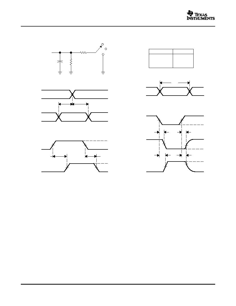
Figure 4. Load Circuit and Voltage Waveforms
12

www.ti.com
PARAMETER MEASUREMENT INFORMATION
V
CC
/2
V
CC
/2
V
CC
/2
V
CC
/2
V
CC
/2
V
CC
/2
V
CC
/2
V
CC
/2
V
OH
V
OL
t
h
t
su
From Output
Under Test
C
L
= 30 pF
(see Note A)
LOAD CIRCUIT
S1
Open
GND
500
500
Output
Control
(low-level
enabling)
Output
Waveform 1
S1 at 2
×
V
CC
(see Note B)
Output
Waveform 2
S1 at GND
(see Note B)
t
PZL
t
PZH
t
PLZ
t
PHZ
0 V
V
OL
+ 0.15 V
V
OH
- 0.15 V
0 V
V
CC
0 V
0 V
t
w
V
CC
V
CC
VOLTAGE WAVEFORMS
SETUP AND HOLD TIMES
VOLTAGE WAVEFORMS
PULSE DURATION
VOLTAGE WAVEFORMS
ENABLE AND DISABLE TIMES
Timing
Input
Data
Input
Input
t
pd
t
PLZ
/t
PZL
t
PHZ
/t
PZH
Open
2
×
V
CC
GND
TEST
S1
NOTES: A. C
L
includes probe and jig capacitance.
B. Waveform 1 is for an output with internal conditions such that the output is low, except when disabled by the output control.
Waveform 2 is for an output with internal conditions such that the output is high, except when disabled by the output control.
C. All input pulses are supplied by generators having the following characteristics: PRR
10 MHz, Z
O
= 50
, t
r
2 ns, t
f
2 ns.
D. The outputs are measured one at a time, with one transition per measurement.
E. t
PLZ
and t
PHZ
are the same as t
dis
.
F. t
PZL
and t
PZH
are the same as t
en
.
G. t
PLH
and t
PHL
are the same as t
pd
.
0 V
V
CC
V
CC
/2
t
PHL
V
CC
/2
V
CC
/2
V
CC
0 V
V
OH
V
OL
Input
Output
VOLTAGE WAVEFORMS
PROPAGATION DELAY TIMES
V
CC
/2
V
CC
/2
t
PLH
2
×
V
CC
V
CC
SN74AVC16646
16-BIT BUS TRANSCEIVER AND REGISTER
WITH 3-STATE OUTPUTS
SCES181F DECEMBER 1998 REVISED JUNE 2005
V
CC
= 2.5 V ± 0.2 V
Figure 5. Load Circuit and Voltage Waveforms
13

www.ti.com
PARAMETER MEASUREMENT INFORMATION
t
PHZ
t
PLH
t
PHL
V
OH
V
OL
t
h
t
su
From Output
Under Test
C
L
= 30 pF
(see Note A)
LOAD CIRCUIT
S1
2
×
V
CC
Open
GND
500
500
Output
Control
(low-level
enabling)
Output
Waveform 1
S1 at 2
×
V
CC
(see Note B)
Output
Waveform 2
S1 at GND
(see Note B)
t
PZL
t
PZH
t
PLZ
V
CC
0 V
V
OH
V
OL
0 V
V
OL
+ 0.3 V
V
OH
- 0.3 V
0 V
V
CC
0 V
0 V
V
CC
0 V
t
w
Input
V
CC
V
CC
V
CC
VOLTAGE WAVEFORMS
SETUP AND HOLD TIMES
VOLTAGE WAVEFORMS
PROPAGATION DELAY TIMES
VOLTAGE WAVEFORMS
PULSE DURATION
VOLTAGE WAVEFORMS
ENABLE AND DISABLE TIMES
Timing
Input
Data
Input
Output
Input
t
pd
t
PLZ
/t
PZL
t
PHZ
/t
PZH
Open
2
×
V
CC
GND
TEST
S1
NOTES: A. C
L
includes probe and jig capacitance.
B. Waveform 1 is for an output with internal conditions such that the output is low, except when disabled by the output control.
Waveform 2 is for an output with internal conditions such that the output is high, except when disabled by the output control.
C. All input pulses are supplied by generators having the following characteristics: PRR
10 MHz, Z
O
= 50
, t
r
2 ns, t
f
2 ns.
D. The outputs are measured one at a time, with one transition per measurement.
E. t
PLZ
and t
PHZ
are the same as t
dis
.
F. t
PZL
and t
PZH
are the same as t
en
.
G. t
PLH
and t
PHL
are the same as t
pd
.
V
CC
/2
V
CC
/2
V
CC
/2
V
CC
/2
V
CC
/2
V
CC
/2
V
CC
/2
V
CC
/2
V
CC
/2
V
CC
/2
V
CC
/2
V
CC
/2
V
CC
/2
SN74AVC16646
16-BIT BUS TRANSCEIVER AND REGISTER
WITH 3-STATE OUTPUTS
SCES181F DECEMBER 1998 REVISED JUNE 2005
V
CC
= 3.3 V ± 0.3 V
Figure 6. Load Circuit and Voltage Waveforms
14

PACKAGING INFORMATION
Orderable Device
Status
(1)
Package
Type
Package
Drawing
Pins Package
Qty
Eco Plan
(2)
Lead/Ball Finish
MSL Peak Temp
(3)
74AVC16646DGGRE4
ACTIVE
TSSOP
DGG
56
2000 Green (RoHS &
no Sb/Br)
CU NIPDAU
Level-1-260C-UNLIM
74AVC16646DGVRE4
ACTIVE
TVSOP
DGV
56
2000 Green (RoHS &
no Sb/Br)
CU NIPDAU
Level-1-260C-UNLIM
SN74AVC16646DGGR
ACTIVE
TSSOP
DGG
56
2000 Green (RoHS &
no Sb/Br)
CU NIPDAU
Level-1-260C-UNLIM
SN74AVC16646DGVR
ACTIVE
TVSOP
DGV
56
2000 Green (RoHS &
no Sb/Br)
CU NIPDAU
Level-1-260C-UNLIM
(1)
The marketing status values are defined as follows:
ACTIVE: Product device recommended for new designs.
LIFEBUY: TI has announced that the device will be discontinued, and a lifetime-buy period is in effect.
NRND: Not recommended for new designs. Device is in production to support existing customers, but TI does not recommend using this part in
a new design.
PREVIEW: Device has been announced but is not in production. Samples may or may not be available.
OBSOLETE: TI has discontinued the production of the device.
(2)
Eco
Plan
-
The
planned
eco-friendly
classification:
Pb-Free
(RoHS)
or
Green
(RoHS
&
no
Sb/Br)
-
please
check
http://www.ti.com/productcontent
for the latest availability information and additional product content details.
TBD: The Pb-Free/Green conversion plan has not been defined.
Pb-Free (RoHS): TI's terms "Lead-Free" or "Pb-Free" mean semiconductor products that are compatible with the current RoHS requirements
for all 6 substances, including the requirement that lead not exceed 0.1% by weight in homogeneous materials. Where designed to be soldered
at high temperatures, TI Pb-Free products are suitable for use in specified lead-free processes.
Green (RoHS & no Sb/Br): TI defines "Green" to mean Pb-Free (RoHS compatible), and free of Bromine (Br) and Antimony (Sb) based flame
retardants (Br or Sb do not exceed 0.1% by weight in homogeneous material)
(3)
MSL, Peak Temp. -- The Moisture Sensitivity Level rating according to the JEDEC industry standard classifications, and peak solder
temperature.
Important Information and Disclaimer:The information provided on this page represents TI's knowledge and belief as of the date that it is
provided. TI bases its knowledge and belief on information provided by third parties, and makes no representation or warranty as to the
accuracy of such information. Efforts are underway to better integrate information from third parties. TI has taken and continues to take
reasonable steps to provide representative and accurate information but may not have conducted destructive testing or chemical analysis on
incoming materials and chemicals. TI and TI suppliers consider certain information to be proprietary, and thus CAS numbers and other limited
information may not be available for release.
In no event shall TI's liability arising out of such information exceed the total purchase price of the TI part(s) at issue in this document sold by TI
to Customer on an annual basis.
PACKAGE OPTION ADDENDUM
www.ti.com
5-Sep-2005
Addendum-Page 1

MECHANICAL DATA
MPDS006C FEBRUARY 1996 REVISED AUGUST 2000
POST OFFICE BOX 655303
·
DALLAS, TEXAS 75265
DGV (R-PDSO-G**)
PLASTIC SMALL-OUTLINE
24 PINS SHOWN
14
3,70
3,50
4,90
5,10
20
DIM
PINS **
4073251/E 08/00
1,20 MAX
Seating Plane
0,05
0,15
0,25
0,50
0,75
0,23
0,13
1
12
24
13
4,30
4,50
0,16 NOM
Gage Plane
A
7,90
7,70
38
24
16
4,90
5,10
3,70
3,50
A MAX
A MIN
6,60
6,20
11,20
11,40
56
9,60
9,80
48
0,08
M
0,07
0,40
0
°
8
°
NOTES: A. All linear dimensions are in millimeters.
B. This drawing is subject to change without notice.
C. Body dimensions do not include mold flash or protrusion, not to exceed 0,15 per side.
D. Falls within JEDEC: 24/48 Pins MO-153
14/16/20/56 Pins MO-194

MECHANICAL DATA
MTSS003D JANUARY 1995 REVISED JANUARY 1998
POST OFFICE BOX 655303
·
DALLAS, TEXAS 75265
DGG (R-PDSO-G**)
PLASTIC SMALL-OUTLINE PACKAGE
4040078 / F 12/97
48 PINS SHOWN
0,25
0,15 NOM
Gage Plane
6,00
6,20
8,30
7,90
0,75
0,50
Seating Plane
25
0,27
0,17
24
A
48
1
1,20 MAX
M
0,08
0,10
0,50
0
°
8
°
56
14,10
13,90
48
DIM
A MAX
A MIN
PINS **
12,40
12,60
64
17,10
16,90
0,15
0,05
NOTES: A. All linear dimensions are in millimeters.
B. This drawing is subject to change without notice.
C. Body dimensions do not include mold protrusion not to exceed 0,15.
D. Falls within JEDEC MO-153

IMPORTANT NOTICE
Texas Instruments Incorporated and its subsidiaries (TI) reserve the right to make corrections, modifications,
enhancements, improvements, and other changes to its products and services at any time and to discontinue
any product or service without notice. Customers should obtain the latest relevant information before placing
orders and should verify that such information is current and complete. All products are sold subject to TI's terms
and conditions of sale supplied at the time of order acknowledgment.
TI warrants performance of its hardware products to the specifications applicable at the time of sale in
accordance with TI's standard warranty. Testing and other quality control techniques are used to the extent TI
deems necessary to support this warranty. Except where mandated by government requirements, testing of all
parameters of each product is not necessarily performed.
TI assumes no liability for applications assistance or customer product design. Customers are responsible for
their products and applications using TI components. To minimize the risks associated with customer products
and applications, customers should provide adequate design and operating safeguards.
TI does not warrant or represent that any license, either express or implied, is granted under any TI patent right,
copyright, mask work right, or other TI intellectual property right relating to any combination, machine, or process
in which TI products or services are used. Information published by TI regarding third-party products or services
does not constitute a license from TI to use such products or services or a warranty or endorsement thereof.
Use of such information may require a license from a third party under the patents or other intellectual property
of the third party, or a license from TI under the patents or other intellectual property of TI.
Reproduction of information in TI data books or data sheets is permissible only if reproduction is without
alteration and is accompanied by all associated warranties, conditions, limitations, and notices. Reproduction
of this information with alteration is an unfair and deceptive business practice. TI is not responsible or liable for
such altered documentation.
Resale of TI products or services with statements different from or beyond the parameters stated by TI for that
product or service voids all express and any implied warranties for the associated TI product or service and
is an unfair and deceptive business practice. TI is not responsible or liable for any such statements.
Following are URLs where you can obtain information on other Texas Instruments products and application
solutions:
Products
Applications
Amplifiers
amplifier.ti.com
Audio
www.ti.com/audio
Data Converters
dataconverter.ti.com
Automotive
www.ti.com/automotive
DSP
dsp.ti.com
Broadband
www.ti.com/broadband
Interface
interface.ti.com
Digital Control
www.ti.com/digitalcontrol
Logic
logic.ti.com
Military
www.ti.com/military
Power Mgmt
power.ti.com
Optical Networking
www.ti.com/opticalnetwork
Microcontrollers
microcontroller.ti.com
Security
www.ti.com/security
Telephony
www.ti.com/telephony
Video & Imaging
www.ti.com/video
Wireless
www.ti.com/wireless
Mailing Address:
Texas Instruments
Post Office Box 655303 Dallas, Texas 75265
Copyright
2005, Texas Instruments Incorporated