LTC3425
1
3425p
s
Handheld Computers
s
Point-of-Load Regulators
s
3.3V to 5V Conversion
, LTC and LT are registered trademarks of Linear Technology Corporation.
s
High Efficiency: Up to 95%
s
Up to 3A Continuous Output Current
s
4-Phase Operation for Low Output Ripple
and Tiny Solution Size
s
Output Disconnect and Inrush Current Limiting
s
Very Low Quiescent Current: 12
µ
A
s
0.5V to 4.5V Input Range
s
2.4V to 5.25V Adjustable Output Voltage
s
Adjustable Current Limit
s
Adjustable, Fixed Frequency Operation from
100kHz to 2MHz per Phase
s
Synchronizable Oscillator with Sync Output
s
Internal Synchronous Rectifiers
s
Manual or Automatic Burst Mode
®
Operation
s
Power Good Comparator
s
<1
µ
A Shutdown Current
s
Antiringing Control
s
5mm
×
5mm Thermally Enhanced QFN Package
5A, 8MHz, 4-Phase
Synchronous Step-Up DC/DC Converter
June 2003
FEATURES
DESCRIPTIO
U
APPLICATIO S
U
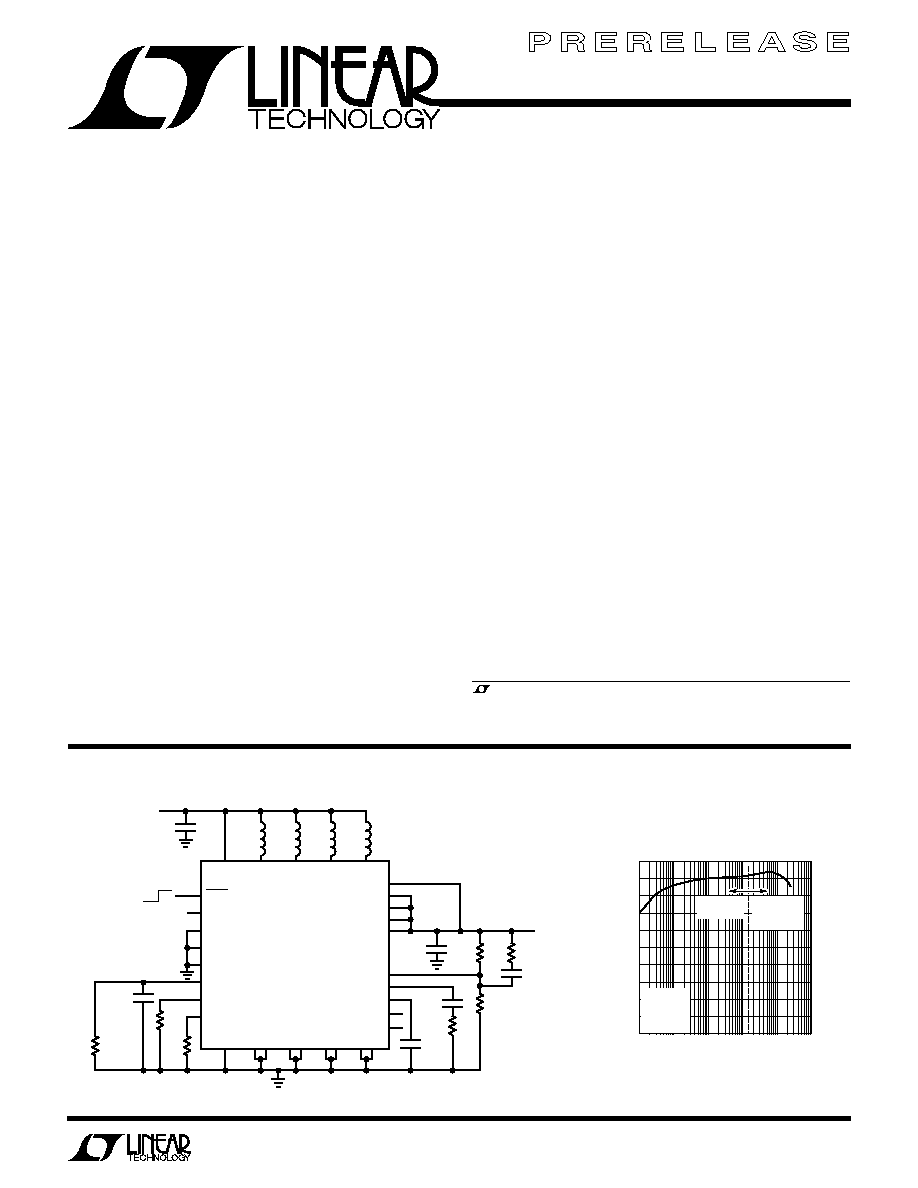
TYPICAL APPLICATIO
U
Information furnished by Linear Technology Corporation is believed to be accurate and reliable.
However, no responsibility is assumed for its use. Linear Technology Corporation makes no represen-
tation that the interconnection of its circuits as described herein will not infringe on existing patent rights.
Burst Mode is a registered trademark of Linear Technology Corporation.
The LTC
®
3425 is a synchronous, 4-phase boost converter
with output disconnect capable of operation below 1V
input. It includes four N-channel MOSFET switches and
four P-channel synchronous rectifiers for an effective
R
DS(ON)
of 0.045
and 0.05
, respectively. 4-phase
operation greatly reduces peak inductor currents, capaci-
tor ripple current and increases effective switching fre-
quency, minimizing inductor and capacitor sizes. True
output disconnect eliminates inrush current and allows
zero load current in shutdown. External Schottky diodes
are not required in most applications (V
OUT
< 4.3V). Power
saving Burst Mode operation can be user controlled or left
in automatic mode.
Other features include 1
µ
A shutdown current, program-
mable frequency with sync in and out, programmable
soft-start, antiringing control, thermal shutdown, adjust-
able current limit, reference output and power good
comparator.
The LTC3425 is available in a small, thermally enhanced
32-pin QFN package.
2.7
µ
H
2.2
µ
F
0.01
µ
F
75k
15k
20k
2.7
µ
H
2.7
µ
H
2.7
µ
H
C
IN
: TAIYO YUDEN JMK107BJ225MA
C
OUT
: TAIYO YUDEN JMK212BJ475MG (
×
4)
L1-L4: TDK RLF5018T-2R7M1R8
V
IN
SWA
V
IN
2V TO 3V
SWB
LTC3425
SWC
SWD
SGND
SHDN
OFF ON
V
OUTS
V
OUTA
V
OUTB
V
OUTC
V
OUTD
REFOUT
CCM
REFEN
SYNCIN
BURST
R
T
I
LIM
PGOOD
SYNCOUT
SS
FB
COMP
GNDA
GNDB
GNDC
GNDD
330pF
22pF
3425 TA01
4.7
µ
F
×
4
0.01
µ
F
33k
590k
1M
10k
V
OUT
3.3V
2A
LOAD CURRENT (mA)
0.1
70
EFFICIENCY (%)
80
90
1
10
100
1000
10000
3425 TA02
60
50
40
30
20
10
0
100
V
IN
= 2.4V
V
OUT
= 3.3V
f = 1MHz
L = 2.7
µ
H
Burst Mode
OPERATION
FIXED
FREQUENCY
MODE
Electrical Specifications Subject to Change

LTC3425
2
3425p
PARAMETER
CONDITIONS
MIN
TYP
MAX
UNITS
Minimum Start-Up Voltage
V
OUT
= 0V, I
LOAD
< 1mA
0.88
1
V
Minimum Operating Voltage
SHDN > 0.65V (Note 3)
q
0.5
V
Output Voltage Adjust Range
q
2.4
5.25
V
Feedback Regulation Voltage
q
1.196
1.220
1.244
V
Feedback Input Current
V
FB
= 1.25V
1
50
nA
V
OUT
Quiescent Current--Burst Mode Operation
BURST = 0V, REFEN = 0V, FB = 1.3V (Note 2)
12
25
µ
A
BURST = 0V, REFEN = 2V, FB = 1.3V (Note 2)
18
35
µ
A
V
IN
Quiescent Current--Shutdown
SHDN = 0V, V
OUT
= 0V, Not Including Switch Leakage
0.1
1
µ
A
V
OUT
Quiescent Current--Active
V
C
= 0V, Nonswitching (Note 2)
1.8
mA
NMOS Switch Leakage
V
SW
= 5V
0.1
5
µ
A
PMOS Switch Leakage
V
SW
= 5V, V
OUT
= 0V
0.1
10
µ
A
NMOS Switch On Resistance
(Note 4)
0.045
PMOS Switch On Resistance
(Note 4)
0.05
NMOS Current Limit
I
LIM
Resistor = 75k (Note 4)
q
5.0
7.0
A
I
LIM
Resistor = 200k (Note 4)
q
1.8
2.7
A
V
IN
Voltage ................................................. 0.3V to 6V
SWA-D Voltages
DC .......................................................... 0.3V to 6V
Pulsed < 100ns ...................................... 0.3V to 7V
V
OUTA-D
, V
OUTS
Voltages............................ 0.3V to 6V
BURST, SHDN, SS, REFEN, SYNCOUT, PGOOD,
CCM, SYNCIN Voltages .............................. 0.3V to 6V
Operating Temperature Range (Note 5) ... 40
°
C to 85
°
C
Storage Temperature Range ................. 65
°
C to 125
°
C
Lead Temperature (Soldering, 10 sec).................. 300
°
C
ORDER PART
NUMBER
Consult LTC Marketing for parts specified with wider operating temperature ranges.
LTC3425EUH
ABSOLUTE AXI U
RATI GS
W
W
W
U
PACKAGE/ORDER I FOR ATIO
U
U
W
(Note 1)
T
JMAX
= 125
°
C,
JA
= 40
°
C/W 1 LAYER BOARD,
JA
= 35
°
C/W 4 LAYER BOARD
EXPOSED PAD IS ???? (PIN 33) MUST BE SOLDERED TO PCB
32 31 30 29 28 27 26 25
9
10 11 12
TOP VIEW
33
UH PACKAGE
32-LEAD (5mm
×
5mm) PLASTIC QFN
13 14 15 16
17
18
19
20
21
22
23
24
8
7
6
5
4
3
2
1
GNDA
GNDA
SWA
V
OUTA
V
OUTB
SWB
GNDB
GNDB
GNDD
GNDD
SWD
V
OUTD
V
OUTC
SWC
GNDC
GNDC
SS
SHDN
SYNCIN
V
IN
R
T
I
LIM
CCM
SYNCOUT
REFEN
V
OUTS
SGND
FB
COMP
BURST
REFOUT
PGOOD
ELECTRICAL CHARACTERISTICS
The
q
denotes the specifications which apply over the full operating
temperature range, otherwise specifications are at T
A
= 25
°
C. V
IN
= 1.2V, V
OUT
= 3.3V, R
T
= 15k, unless otherwise noted.
UH PART
MARKING
3425

LTC3425
3
3425p
PARAMETER
CONDITIONS
MIN
TYP
MAX
UNITS
PMOS Turn-Off Current
CCM < 0.4V
80
mA
PMOS Current Limit
CCM > 1.4V
0.6
A
Max Duty Cycle
q
83
90
97
%
Min Duty Cycle
q
0
%
Frequency Accuracy
R
T
= 15k
q
0.8
1
1.2
MHz
SHDN Input High
V
OUT
= 0V (Initial Start-Up)
q
1
V
V
OUT
> 2.4V
q
0.65
V
SHDN Input Low
q
0.25
V
SHDN Input Current
V
SHDN
= 0V, 3.3V
0.01
1
µ
A
V
SHDN
= 2V
0.50
µ
A
REFEN, CCM Input High
q
1.4
V
REFEN, CCM Input Low
q
0.4
V
REFEN, Input Current
V
REFEN
= 5V
0.01
1
µ
A
SYNCIN Input High
q
2.5
V
SYNCIN Input Low
q
0.5
V
SYNCIN Input Current
V
SYNCIN
= 5V
0.3
1
µ
A
CCM Input Current
V
CCM
= 5V
1.7
4
µ
A
SYNC Input Pulse Width
q
0.1
µ
s
SYNC Out High
3
V
SYNC Out Low
0.4
V
REFOUT
REFEN > 1.4V, No Load
q
1.190
1.220
1.251
V
REFOUT
I
SOURCE
< 100
µ
A, I
SINK
< 10
µ
A, REFEN > 1.4V
q
1.184
1.22
1.252
V
Error Amp Transconductance
50
µ
S
Error Amp Output High
I
LIM
Resistor = 75k
2.2
V
Error Amp Output Low
0.15
V
PGOOD Threshold (Falling Edge)
Referenced to Feedback Voltage
q
9.5
11.4
13.5
%
PGOOD Hysteresis
Referenced to Feedback Voltage
q
1.5
2.5
3.5
%
PGOOD Low Voltage
I
SINK
= 1mA (10mA Max)
q
0.12
0.25
V
PGOOD Leakage
V
PGOOD
= 5.5V
q
0.01
1
µ
A
SS Current Source
V
SS
= 1V
q
2.5
µ
A
Burst Threshold Voltage (Falling Edge)
q
0.84
0.94
1.04
V
Burst Threshold Hysteresis
115
mV
ELECTRICAL CHARACTERISTICS
The
q
denotes the specifications which apply over the full operating
temperature range, otherwise specifications are at T
A
= 25
°
C. V
IN
= 1.2V, V
OUT
= 3.3V, R
T
= 15k, unless otherwise noted.
Note 1: Absolute Maximum Ratings are those values beyond which the life
of a device may be impaired.
Note 2: Current is measured into the V
OUTS
pin since the supply current is
bootstrapped to the output. The current will reflect to the input supply by
V
OUT
/(V
IN
· Efficiency). The outputs are not switching.
Note 3: Once the output is started, the IC is not dependent on the V
IN
supply as long as SHDN > 0.65V.
Note 4: Total with all four FETs in parallel.
Note 5: The LTC3425E is guaranteed to meet performance specifications
from 0
°
C to 70
°
C. Specifications over the 40
°
C to 85
°
C operating
temperature range are assured by design, characterization and correlation
with statistical process controls.
Note 6: This IC includes overtemperature protection that is intended to
protect the device during momentary overload conditions. Junction
temperature will exceed 125
°
C when overtemperature protection is active.
Continuous operation above the specified maximum operating junction
temperature may result in device degradation or failure.

LTC3425
4
3425p
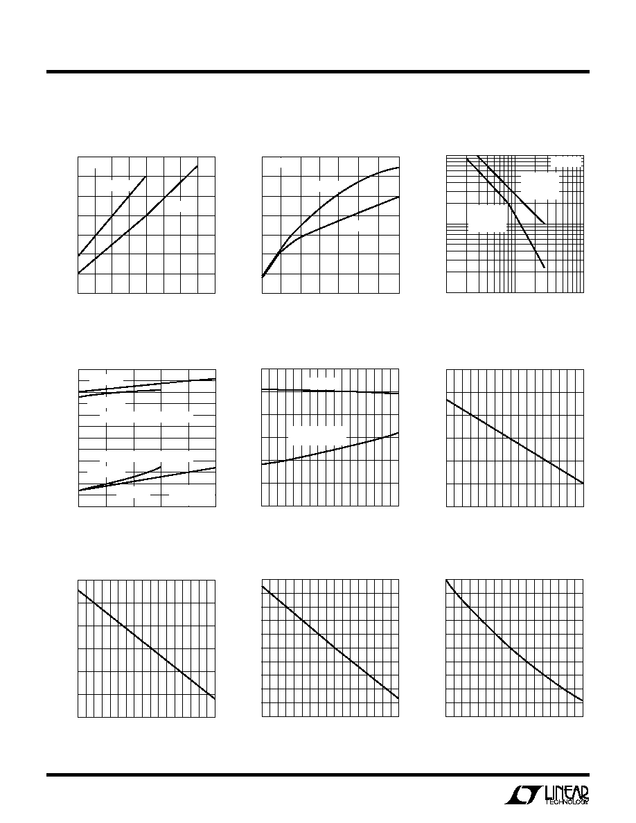
TYPICAL PERFOR A CE CHARACTERISTICS
U
W
SWA, SWB, SWC, SWD
at 1MHz/Phase
SW Pin and Oscillator SYNCOUT
SW Pin and Inductor Current in
Discontinous Mode. Antiring
Circuit Eliminates High Frequency
Ringing
Transient Response 0.5A to 1.5A
Fixed Frequency Mode Operation
Output Voltage Ripple at 2.5A
Load with Only Four 4.7
µ
F
Ceramic Capacitors
Soft-Start and Inrush Current
Limiting
Burst Mode Operation
SWA TO SWD
5V/DIV
250ns/DIV
3425 G01
SWA
2V/DIV
250ns/DIV
3425 G02
SYNCOUT
2V/DIV
V
IN
= 2.4V
250ns/DIV
3425 G03
V
OUT
= 3.3V
C
OUT
= 220
µ
F
I
L
0.2A/DIV
SW
2V/DIV
V
IN
= 2.4V
100
µ
s/DIV
3425 G04
V
OUT
= 3.3V
C
OUT
= 220
µ
F
V
OUT
AC
100mV/DIV
LOAD
CURRENT
0.5A/DIV
V
IN
= 2.4V
500ns/DIV
3425 G05
V
OUT
= 3.3V
FREQUENCY = 1MHz/PHASE
V
OUT
AC
50mV/DIV
Output Voltage Ripple at 2.5A
Load with a 47
µ
F Ceramic Bulk
Capacitor
V
IN
= 2.4V
500ns/DIV
3425 G06
V
OUT
= 3.3V
FREQUENCY = 1MHz/PHASE
V
OUT
AC
10mV/DIV
V
IN
= 2.4V
500
µ
s/DIV
3425 G07
V
OUT
= 3.3V
C
SOFTSTART
= 0.015
µ
F
I
IN
0.5A/DIV
SS Pin
1V/DIV
V
OUT
2V/DIV
V
IN
= 2.4V
25
µ
s/DIV
3425 G08
V
OUT
= 3.3V
C
OUT
= 220
µ
F
SWA
2V/DIV
V
OUT
AC
50mV/DIV
Transient Response 10mA to 1A
Automatic Burst Mode Operation
V
IN
= 2.4V
1ms/DIV
3425 G10
V
OUT
= 3.3V
C
OUT
= 220
µ
F
I
OUT
1A/DIV
BURST PIN
1V/DIV
V
OUT
AC
200mV/DIV

LTC3425
5
3425p
TYPICAL PERFOR A CE CHARACTERISTICS
U
W
Converter Efficiency
for V
OUT
= 3.3V
Converter Efficiency for 2-, 3- and
4-Phase Operation
Efficiency Comparison of
Discontinuous Mode and Forced
Continuous Mode at Light Loads
for V
IN
= 2.4V, V
OUT
= 3.3V
Converter No Load Input Current
vs V
IN
(Burst Mode Operation)
Oscillator Frequency
Peak Current Limit
OUTPUT CURRENT (mA)
0.1
1
70
EFFICIENCY (%)
80
90
10
100
1000
10000
3425 G11
60
50
40
30
20
10
0
100
V
IN
= 2.4V
V
IN
= 1.2V
V
IN
= 1.2V
V
IN
= 2.4V
T
J
= 25
°
C
Burst Mode OPERATION
1MHz/PHASE
OUTPUT CURRENT (mA)
0.1
1
70
EFFICIENCY (%)
80
90
10
100
1000
10000
3425 G12
60
0
10
20
30
40
50
100
T
J
= 25
°
C
V
IN
= 3.3V
V
IN
= 3.3V
V
IN
= 2.4V
V
IN
= 2.4V
Burst Mode OPERATION
1MHz/PHASE
Converter Efficiency
for V
OUT
= 5V
LOAD (mA)
100
80
EFFICIENCY (%)
84
82
86
88
90
92
94
96
1000
10000
3425 G13
98
4 PHASE
T
J
= 25
°
C
V
IN
= 2.4V
V
OUT
= 3.3V
3 PHASE
2 PHASE
CONVERTER OUTPUT CURRENT (mA)
1
40
EFFICIENCY (%)
50
60
70
80
10
100
1000
3425 G14
30
20
10
0
90
100
T
J
= 25
°
C
DISCONTINUOUS
MODE
FORCED
CONTINUOUS
MODE
LOAD (mA)
1
40
EFFICIENCY (%)
50
60
70
80
10
100
1000
3425 G15
30
20
10
0
90
100
T
J
= 25
°
C
DISCONTINUOUS
MODE
FORCED
CONTINUOUS
MODE
Efficiency Comparison of
Discontinuous Mode and Forced
Continuous Mode at Light Loads
for V
IN
= 3.3V, V
OUT
= 5V
V
IN
(V)
1.5
140
120
100
80
60
40
20
0
3.0
4.0
3425 G16
2.0
2.5
3.5
4.5
CONVERTER INPUT CURRENT (
µ
A)
T
J
= 25
°
C
V
OUT
= 3.3V
V
OUT
= 5V
R
T
(k
)
1
1
FREQUENCY (MHz)
10
10
100
3425 G17
T
J
= 25
°
C
I
LIM
RESISTOR (k
)
60
PEAK CURRENT IN EACH PHASE (A)
1.4
1.6
1.8
120
160
3425 G18
1.2
1.0
80
100
140
180
200
0.8
0.6
T
J
= 25
°
C
Effective R
DS(ON)
V
OUT
(V)
2.5
R
DS(ON)
(ALL FOUR PHASES IN PARALLEL)
0.065
0.060
0.055
0.050
0.045
0.040
4.5
3425 G19
3
3.5
4
5
T
J
= 25
°
C
PMOS
NMOS
LTC3425
6
3425p
TYPICAL PERFOR A CE CHARACTERISTICS
U
W
Maximum Output Current
in Burst Mode Operation
V
IN
(V)
1
1.5
OUTPUT CURRENT (mA)
200
250
300
4
3425 G20
150
100
2
3
4.5
2.5
3.5
5
50
0
350
V
OUT
= 3.3V
V
OUT
= 5V
T
J
= 25
°
C
V
IN
(V)
0.9
0.4
0.5
0.7
1.2
1.4
3425 G21
0.3
0.2
1.0
1.1
1.3
1.5
1.6
0.1
0
0.6
LOAD CURRENT (A)
T
J
= 25
°
C
V
OUT
= 3.3V
V
OUT
= 5V
Maximum Start-Up Load vs V
IN
(Constant Current Load)
Soft-Start Charging Current
vs Temperature
Automatic Burst Mode Current
Thresholds vs R
BURST
BURST RESISTOR (k
)
10
1
AVERAGE LOAD CURRENT (mA)
10
100
100
1000
3425 G22
T
J
= 25
°
C
ENTER
Burst Mode
OPERATION
LEAVE
Burst Mode
OPERATION
V
IN
(V)
1.5
LOAD CURRENT (mA)
70
80
90
100
3.5
3425 G23
60
50
40
2
2.5
3
4
V
OUT
= 5V
T
J
= 25
°
C
R
BURST
= 33k
V
OUT
= 5V
V
OUT
= 3.3V
LEAVE Burst Mode OPERATION
ENTER Burst Mode OPERATION
V
OUT
= 3.3V
TEMPERATURE (
°
C)
45
0
SS CHARGE CURRENT (
µ
A)
0.5
1.0
1.5
2.0
3.0
25
5
15
35
75
55
3425 G24
95
115
2.5
V
IN
> 2.3V
V
IN
< 2.3V
(START-UP MODE)
Automatic Burst Mode Thresholds
vs V
IN
PGOOD Threshold vs Temperature
Shutdown Voltage vs Temperature
Minimum Start-Up Voltage
vs Temperature
TEMPERATURE (
°
C)
45
0.300
SHUTDOWN VOLTAGE (V)
0.325
0.350
0.375
0.400
0.450
25
5
15
35
75
55
3425 G25
95
115
0.425
TEMPERATURE (
°
C)
45
0.70
START VOLTAGE (V)
0.75
0.80
0.85
0.90
1.00
25
5
15
35
75
55
3425 G26
95
115
0.95
TEMPERATURE (
°
C)
45
10.8
PGOOD THRESHOLD (1% BELOW V
FB
)
11.0
10.9
11.1
11.5
11.4
11.3
11.2
11.6
11.8
25
5
15
35
75
55
3425 G27
95
115
11.7
PMOS Reverse Current in Forced
CCM vs Temperature
TEMPERATURE (
°
C)
45
300
PMOS REVERSE CURRENT (mA)
400
350
450
650
600
550
500
700
800
25
5
15
35
75
55
3425 G28
95
115
750

LTC3425
7
3425p
TYPICAL PERFOR A CE CHARACTERISTICS
U
W
Feedback Voltage vs Temperature
Peak Current Limit
vs Temperature
Error Amplifier g
m
vs Temperature
Oscillator Frequency
vs Temperature
Burst Mode V
OUT
Quiescent
Current vs Temperature
TEMPERATURE (
°
C)
45
1.200
V
FB
(V)
1.205
1.210
1.215
1.220
1.230
25
5
15
35
75
55
3425 G29
95
115
1.225
TEMPERATURE (
°
C)
45
3
PEAK I
LIM
(NORMALIZED) (%)
2
1
1
0
3
25
5
15
35
75
55
3425 G30
95
115
2
TEMPERATURE (
°
C)
45
2.0
OSCILLATOR (NORMALIZED) (%)
1.5
1.0
0.5
1.0
0.5
0
2.0
25
5
15
35
75
55
3425 G31
95
115
1.5
TEMPERATURE (
°
C)
45
5
QUIESCENT CURRENT (
µ
A)
10
15
20
25
5
15
35
75
55
3425 G32
95
115
TEMPERATURE (
°
C)
45
40
g
m
(
µ
S)
45
50
55
25
5
15
35
75
55
3425 G33
95
115

LTC3425
8
3425p
PI FU CTIO S
U
U
U
GNDAD (Pins 1, 2, 7, 8, 17, 18, 23, 24): Power Ground
for the IC and the Four Internal N-channel MOSFETs.
Connect directly to the power ground plane.
SWAD (Pins 3, 6, 19, 22): Switch Pins. Connect induc-
tors here. Minimize trace length to keep EMI to a mini-
mum. For discontinuous inductor current, a controlled
impedance is internally connected from the SW pins to V
IN
to minimize EMI. For applications where V
OUT
> 4.3V, it is
required to have Schottky diodes from SW to V
OUT
or a
snubber circuit to stay within absolute maximum rating on
the SW pins.
V
OUTAD
(Pins 4, 5, 20, 21): Output of the Four Synchro-
nous Rectifiers. Connect output filter capacitors to these
pins. Connect one low ESR ceramic capacitor directly
from each pin to the ground plane.
REFEN (Pin 9): Pull this pin above 1.4V to enable the REF
output. Grounding this pin turns the REF output off to
reduce quiescent current.
V
OUTS
(Pin 10): V
OUT
Sense Pin. Connect V
OUTS
directly to
an output filter capacitor. The top of the feedback divider
network should also be tied to this point.
SGND (Pin 11): Signal Ground Pin. Connect to ground
plane, near the feedback divider resistor.
FB (Pin 12): Feedback Pin. Connect FB to a resistor divider,
keeping the trace as short as possible. The output voltage
can be adjusted according to the following formula:
V
R
R
R
OUT
=
+
1 22
1
2
1
.
·
where R1 is connected from FB to SGND and R2 is
connected from FB to V
OUTS
.
COMP (Pin 13): Error Amp Output. A frequency compen-
sation network is connected from this pin to ground to
compensate the loop. See the section Closing the Feed-
back Loop for guidelines.
BURST (Pin 14): Burst Mode Threshold Adjust Pin. A
resistor/capacitor combination from this pin to ground
programs the average load current at which automatic
Burst Mode operation is entered.
For manual control of Burst Mode operation, ground the
BURST pin to force Burst Mode operation or connect it to
V
OUT
to force fixed frequency PWM mode. Note that the
BURST pin must not be pulled higher than V
OUT
.
REFOUT (Pin 15): Buffered 1.22V Reference Output. This
pin can source up to 100
µ
A and sink up to 10
µ
A (only
active when the REFEN pin is pulled high). This pin must
be decoupled with a 0.1
µ
F capacitor for stability.
PGOOD (Pin 16): Open-Drain Output of the Power Good
Comparator. This pin will go low when the output voltage
drops 11% below its regulated value. Maximum sink
current should be limited to 10mA.
SYNCOUT (Pin 25): Sync Output Pin. A clock is provided
at the oscillator frequency, but phase-shifted 180 degrees
to allow for synchronizing two devices for an 8-phase
converter.
CCM (Pin 26): This pin is used to select forced continuous
conduction mode. Normally this pin is grounded to allow
CCM or DCM operation. To force continuous conduction
mode, tie this pin to V
OUT
. In this mode, a reverse current
of up to about 0.5A will be allowed before turning off the
synchronous rectifier. This will prevent pulse skipping at
light load when Burst Mode operation is disabled, and will
also improve the large-signal transient response when
going from a heavy load to a light load. For Burst Mode
operation, the CCM pin should be low.

LTC3425
9
3425p
I
LIM
(Pin 27): Current Limit Adjust Pin. Connect a resistor
from I
LIM
to SGND to set the peak current limit threshold
for the N-channel MOSFETs, according to the formula
(note that this is the peak current in each inductor):
I
R
LIM
=
130
where I is in Amps and R is in k
. Do not use values less
than 75k.
R
T
(Pin 28): Connect a resistor from R
T
to SGND (or SGND
plane) to program the oscillator frequency, according to
the formula:
f
R
f
f
R
OSC
T
SWITCH
OSC
T
=
=
=
60
4
15
where f
OSC
is in MHz and R
T
is in k
.
V
IN
(Pin 29): Input Supply Pin. Connect this to the input
supply and decouple with 1
µ
F minimum low ESR
ceramic capacitor.
PI FU CTIO S
U
U
U
SYNCIN (Pin 30): Oscillator Synchronization Pin. A clock
pulse width of 100ns minimum is required to synchronize
the internal oscillator. If not used, SYNCIN should be
grounded. The typical logic threshold for this input is:
V
OUT
2
SHDN (Pin 31): Shutdown Pin. Grounding SHDN (or
pulling it below 0.25V) shuts down the IC. Pull pin up to
1V to enable. Once enabled, the pin only needs to be
0.65V.
SS (Pin 32): Soft-Start pin. Connect a capacitor from this
pin to ground to set the soft-start time, according to the
formula:
t(ms) = C
SS
(
µ
F) · 320
The nominal soft-start charging current is 2.5
µ
A. The
active range of SS is from 0.8V to 1.6V. Note that this is the
rise time of the SS pin. The actual rise time of V
OUT
will be
a function of load and output capacitance.
OPERATING MODE
BURST PIN
CCM PIN
Automatic Burst (Operating Mode is Load Dependent)
RC Network to Ground
Low
Forced Burst
Low
Low
Forced Fixed Frequency with Pulse Skipping at Light Load
High
Low
Forced Fixed Frequency, Low Noise (No Pulse Skipping)
High
High
LTC3425
10
3425p
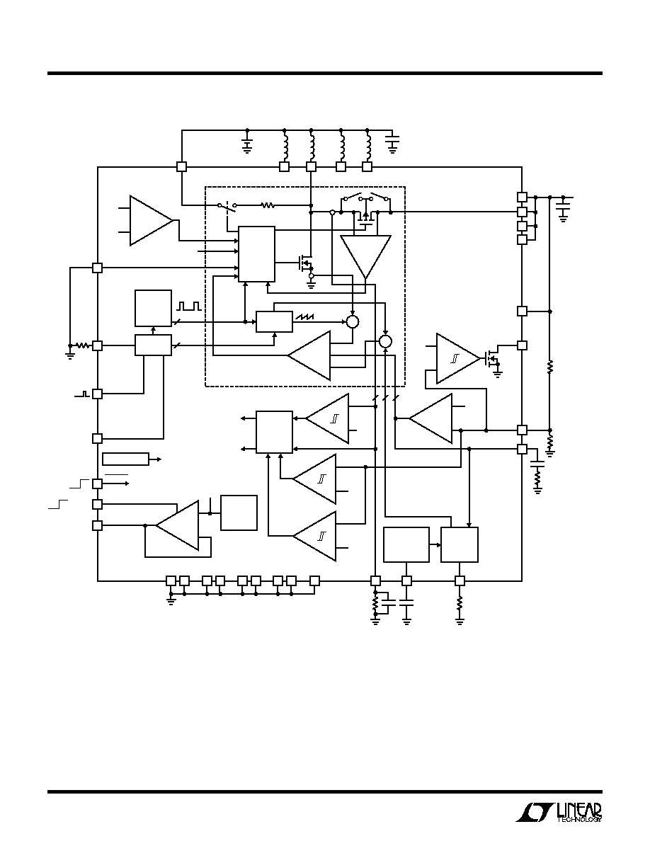
BLOCK DIAGRA
W
3%
0.94V
MODE
SLEEP
V
REF
3%
SGND
GNDD
GNDC
GNDB
GNDA
+
+
Burst Mode
CONTROL
+
+
BURST
COMP
UV
OV
ERROR
AMP
START-UP,
SOFT-START
AND
THERMAL REG
I
LIMIT
COMP
1.22V
1.086/
1.116
+
+
+
+
V
REF
1.22V
I
LIM
27
SS
32
BURST
14
24
23
18
17
8
7
2
1
REFOUT
15
REFEN
SHUTDOWN
9
SHDN
SYNCOUT
SYNCIN
SYNC
OFF ON 31
25
30
R
T
28
CCM
MODE CONTROL
PMOS
ENABLE
FB
0.8V
+
11
THERMAL SHDN
13
FB
12
PGOOD
16
V
OUTS
V
OUT
2.5V TO 5V
10
V
OUTB
5
V
OUTC
20
V
OUTA
4
V
OUTD
21
+
SLOPE
DIVIDER
4-PHASE
GEN
PWM LOGIC
AND
DRIVERS
ANTIRING
N
P
ZERO
I/2000
1V TO V
OUT
1 OF 4
+
OSC
IOSC
CLK
4
4
26
SWB
6
V
IN
+
SWA
29
3
SWC
19
SWD
22
+
4
4
4
+
OFF ON REFOUT

LTC3425
11
3425p
OPERATIO
U
DETAILED DESCRIPTION
The LTC3425 provides high efficiency, low noise power
for high current boost applications such as cellular phones
and PDAs. The true output disconnect feature eliminates
inrush current and allows V
OUT
to go to zero during
shutdown. The current mode architecture with adaptive
slope compensation provides ease of loop compensation
with excellent transient load response. The low R
DS(ON)
,
low gate charge synchronous switches eliminate the need
for an external Schottky rectifier, and provide efficient high
frequency pulse width modulation (PWM) control. High
efficiency is achieved at light loads when Burst Mode
operation is entered, where the IC's quiescent current is a
low 12
µ
A typical on V
OUT
.
MULTIPHASE OPERATION
The LTC3425 uses a 4-phase architecture, rather than the
conventional single phase of other boost converters. By
having multiple phases equally spaced (90
°
apart), not
only is the output ripple frequency increased by a factor of
four, but the output capacitor ripple current is greatly
reduced. Although this architecture requires four induc-
tors, rather than a single inductor, there are a number of
important advantages.
· Much lower peak inductor current allows the use of
smaller, lower cost inductors.
· Greatly reduced output ripple current minimizes output
capacitance requirement.
· Higher frequency output ripple is easier to filter for low
noise applications.
· Input ripple current is also reduced for lower noise on
V
IN
.
The peak boost inductor current is given by:
I
I
D N
di
LPEAK
O
=
+
( ) ·
1
2
Where I
O
is the average load current, D is the PWM duty
cycle, N is the number of phases and di is the inductor
ripple current. This relationship is shown graphically in
Figure 1 using a single phase and a 4-phase example.
Example:
The following example, operating at 50% duty cycle,
illustrates the advantages of multiphase operation over a
conventional single-phase design.
V
IN
= 1.9V, V
OUT
= 3.6V, Efficiency = 90% (approx),
I
OUT
= 2A, Frequency = 1MHz, L = 2.2
µ
H
Table 1
SINGLE
FOUR
CHANGE FROM
PARAMETER
PHASE
PHASE
1 TO 4 PHASE
Peak-Peak Output
4.227A
0.450A
Reduced by 89%
Ripple Current
RMS Output Ripple Current
2.00A
0.184A
Reduced by 91%
Peak Inductor Current
4.227A
1.227A
Reduced by 71%
Output Ripple Frequency
1MHz
4MHz
Increased by 4
×
With 4-phase operation, at least one of the phases will be
delivering current to the load whenever V
IN
is greater than
one quarter V
OUT
(duty cycles less than 75%). For lower
duty cycles, there can be as many as two or three phases
delivering load current simultaneously. This greatly re-
duces both the output ripple current and the peak current
in each inductor, compared with a single-phase converter.
This is illustrated in the waveforms of Figures 2 and 3.
Operation Using Only Two or Three Phases
The LTC3425 can operate as a 2- or 3-phase converter by
simply eliminating the inductor from the unused phase(s).
TIME (
µ
s)
0
OUTPUT RIPPLE CURRENT (A)
2
FOUR PHASE
SINGLE
PHASE
3
3425 F01
1
0
0.5
1
1.5
5
4
Figure 1. Comparison of Output Ripple Current with Single
Phase and 4-Phase Boost Converter in a 2A Load Application
Operating at 50% Duty Cycle

LTC3425
12
3425p
OPERATIO
U
SWITCH A
VOLTAGE
SWITCH B
VOLTAGE
SWITCH C
VOLTAGE
SWITCH D
VOLTAGE
INDUCTOR A
CURRENT
INDUCTOR B
CURRENT
INDUCTOR C
CURRENT
INDUCTOR D
CURRENT
RECTIFIER A
CURRENT
RECTIFIER B
CURRENT
RECTIFIER C
CURRENT
RECTIFIER D
CURRENT
OUTPUT RIPPLE
CURRENT
INPUT CURRENT
3425 F02
Figure 2. Simplified Voltage and Current Waveforms
for 4-Phase Operation at 50% Duty Cycle
This approach can be used to reduce solution cost and
board area in applications not requiring the full power
capability of the LTC3425, or where peak efficiency may
not be as important as cost and size. In this case, phase A
should always be used, since this is the only phase active
in Burst Mode operation and phase C is recommended as
the second phase for the lowest output ripple, since it is
180
°
out of phase with phase A. Figure 4 illustrates the
efficiency differences with two, three and four phases in a
typical 2-cell to 3.3V boost application. In this example,
you can see that for maximum loads less than 1A, the
efficiency penalty for using only two or three phases is
fairly small. Keep in mind, however, that this penalty will
grow larger as the input voltage drops. Output ripple will
also increase with each phase that is eliminated.
Low Voltage Start-Up
The LTC3425 includes an independent start-up oscillator
designed to start up at input voltages as low as 0.88V. The
frequency and peak current limit during start-up are

LTC3425
13
3425p
SWITCH A
VOLTAGE
SWITCH B
VOLTAGE
SWITCH C
VOLTAGE
SWITCH D
VOLTAGE
INDUCTOR A
CURRENT
INDUCTOR B
CURRENT
INDUCTOR C
CURRENT
INDUCTOR D
CURRENT
RECTIFIER A
CURRENT
RECTIFIER B
CURRENT
RECTIFIER C
CURRENT
RECTIFIER D
CURRENT
OUTPUT RIPPLE
CURRENT
INPUT CURRENT
3432 F03
OPERATIO
U
Figure 3. Simplified Voltage and Current Waveforms
for 4-Phase Operation at 75% Duty Cycle
internally controlled. The device can start up under some
load (see the graph Start-Up Current vs Input Voltage).
Soft-start and inrush current limiting is provided during
start-up as well as normal mode. The same soft-start
capacitor is used for each operating mode.
During start-up, all four phases switch in unison. When
either V
IN
or V
OUT
exceeds 2.3V, the IC enters normal
operating mode. Once the output voltage exceeds the
input by 0.3V, the IC powers itself from V
OUT
instead of
V
IN
. At this point the internal circuitry has no dependency
on the V
IN
input voltage, eliminating the requirement for a
large input capacitor. The input voltage can drop as low as
0.5V without affecting circuit operation. The limiting factor
for the application becomes the ability of the power source
to supply sufficient energy to the output at the low volt-
ages, and the maximum duty cycle which is clamped at
90%.

LTC3425
14
3425p
OPERATIO
U
Low Noise Fixed Frequency Operation
Shutdown: The part is shut down by pulling the SHDN pin
below 0.25V and made active by pulling the pin above 1V.
Note that the SHDN pin can be driven above V
IN
or V
OUT
,
as long as it is limited to less than 5.5V.
Soft-Start: The soft-start time is programmed with an
external capacitor to ground on the SS pin. An internal
current source charges it with a nominal 2.5
µ
A (1
µ
A while
in start-up mode when V
IN
and V
OUT
are both below 2.3V).
The voltage on the soft-start pin (in conjunction with the
external resistor on the I
LIM
pin) is used to control the peak
current limit until the voltage on the capacitor exceeds
1.6V, at which point the external resistor sets the peak
current. In the event of a commanded shutdown or a
thermal shutdown, the capacitor is discharged automati-
cally. Note that Burst Mode operation is inhibited during
the soft-start time.
t(ms) = C
SS
(
µ
F) · 320
Oscillator: The frequency of operation is set through a re-
sistor from the R
T
pin to ground. An internally trimmed
timing capacitor resides inside the IC. The internal
oscillator frequency is then divided by four to generate the
four phases, each phase shifted by 90
°
. The oscillator fre-
quency and resulting switching frequency of each of the four
phases are calculated using the following formula:
f
R
f
f
R
OSC
T
SWITCH
OSC
T
=
=
=
60
4
15
where f
OSC
is in MHz and R
T
is in k
.
The oscillator can be synchronized with an external clock
applied to the SYNCIN pin. When synchronizing the oscil-
lator, the free running frequency must be set to an approxi-
mately 30% lower frequency than the desired synchronized
frequency. A SYNCOUT pin is provided for synchronizing
two or more devices. The output sync pulse is 180
°
out of
phase from the internal oscillator, allowing two devices to
be synchronized to create an 8-phase converter. Note that
in Burst Mode operation, the oscillator is turned off and the
SYNCOUT pin is driven low.
In fixed frequency operation, the minimum on-time before
pulse skipping occurs (at light load) is typically 110ns.
Current Sensing: Lossless current sensing converts the
peak current signal to a voltage to sum in with the internal
slope compensation. This summed signal is compared to
the error amplifier output to provide a peak current control
command for the PWM. The slope compensation in the IC
is adaptive to the input and output voltage, therefore the
converter provides the proper amount of slope compensa-
tion to ensure stability, but not an excess to cause a loss
of phase margin in the converter.
Error Amp: The error amplifier is a transconductance
amplifier with its positive input internally connected to the
1.22V reference and its negative input connected to the FB
pin. A simple compensation network is placed from the
COMP pin to ground. Internal clamps limit the minimum
and maximum error amp output voltage for improved
large-signal transient response. During Burst Mode op-
eration, the compensation pin is high impedance, however
clamps limit the voltage on the external compensation
network, preventing the compensation capacitor from
discharging to zero.
Figure 4. LTC3425 Efficiency vs
Load for 2-, 3- and 4-Phase Operation
LOAD (mA)
100
80
EFFICIENCY (%)
84
82
86
88
90
92
94
96
1000
10000
3425 G13
98
4 PHASE
T
J
= 25
°
C
V
IN
= 2.4V
V
OUT
= 3.3V
3 PHASE
2 PHASE

LTC3425
15
3425p
Current Limit: The programmable current limit circuit sets
the maximum peak current in the NMOS switches. The
current limit level is programmed using a resistor to
ground on the I
LIM
pin. Do not use values below 75k. In
Burst Mode operation, the current limit is automatically
set to a nominal value of 0.6A peak for optimal efficiency.
I
R
LIM
=
130
per Phase
where I is in Amps and R is in k
.
Synchronous Rectifier and Zero Current Amp: To pre-
vent the inductor current from running away, the PMOS
synchronous rectifier is only enabled when V
OUT
> (V
IN
+
0.3V) and the FB pin is > 0.8V.The zero current amplifier
monitors the inductor current to the output and shuts off
the synchronous rectifier once the current is below 50mA
typical, preventing negative inductor current. If the CCM
pin is tied high, the amplifier will allow up to 0.6A of
negative current in the synchronous rectifier.
Antiringing Control: The antiringing control connects a
resistor across the inductor to damp the ringing on the SW
pin in discontinuous conduction mode. The LC
SW
ringing
(L = inductor, C
SW
= Capacitance on Switch pin) is low
energy, but can cause EMI radiation.
Power Good: An internal comparator monitors the FB pin
voltage. If the FB pin drops 11.4% below the regulation
value, the PGOOD pin will pull low (sink current should be
limited to 10mA max). The output will stay low until the FB
voltage is within 9.5% of the regulation voltage. A filter
prevents noise spikes from causing nuisance trips.
Reference Output: The internal 1.22V reference is buff-
ered and brought out to the REFOUT pin. It is active when
the REFEN pin is pulled high (above 1.4V). For stability, a
minimum of 0.1
µ
F capacitor must be placed on the REFOUT
pin. The output can source up to 100
µ
A and sink up to
10
µ
A. For the lowest possible quiescent current in Burst
Mode operation, the reference output should be disabled
by grounding the REFEN pin.
Thermal Shutdown: An internal temperature monitor will
start to reduce the programmed peak current limit if the
die temperature exceeds 135
°
C. If the die temperature
continues to rise and reaches 150
°
C, the part will go into
thermal shutdown and all switches will be turned off and
the soft-start capacitor will be reset. The part will be
enabled again when the die temperature has dropped
about 10
°
C. Note: Overtemperature protection is intended
to protect the device during momentary overload condi-
tions. Continuous operation above the specified maxi-
mum operating junction temperature may result in device
degradation or failure.
Burst Mode Operation
Burst Mode operation can be automatic or user controlled.
In automatic operation, the IC will automatically enter
Burst Mode operation at light load and return to fixed
frequency PWM mode for heavier loads. The user can
program the average load current at which the mode
transition occurs using a single resistor.
During Burst Mode operation, only Phase A is active and
the other three phases are turned off, reducing quiescent
current and switching losses by 75%. Note that the
oscillator is also shut down in this mode, since the on time
is determined by the time it takes the inductor current to
reach a fixed peak current, and the off time is determined
by the time it takes for the inductor current to return to
zero.
In Burst Mode operation, the IC delivers energy to the
output until it is regulated and then goes into a sleep mode
where the outputs are off and the IC is consuming only
12
µ
A of quiescent current. In this mode, the output ripple
has a variable frequency component with load current and
will be typically 2% peak-peak. This maximizes efficiency
at very light loads by minimizing switching and quiescent
losses. Burst Mode ripple can be reduced slightly by using
more output capacitance (47
µ
F or greater). This capacitor
does not need to be a low ESR type if low ESR ceramics are
also used. Another method of reducing Burst Mode ripple
is to place a small feedforward capacitor across the upper
resistor in the V
OUT
feedback divider network.
During Burst Mode operation, the COMP pin is discon-
nected from the error amplifier in an effort to hold the
voltage on the external compensation network where it
was before entering Burst Mode operation. To minimize
the effects of leakage current and stray resistance, voltage
clamps limit the min and max voltage on COMP during
OPERATIO
U

LTC3425
16
3425p
Burst Mode operation. This minimizes the transient expe-
rienced when a heavy load is suddenly applied to the
converter after being in Burst Mode operation for an
extended period of time.
For automatic operation, an RC network should be con-
nected from the BURST pin to ground. The value of the
resistor will control the average load current (I
BURST
) at
which Burst Mode operation will be entered and exited
(there is hysteresis to prevent oscillation between modes).
The equation given for the capacitor on the BURST pin is
for the minimum value, to prevent ripple on the BURST pin
from causing the part to oscillate in and out of Burst Mode
operation at the current where the mode transition occurs.
I
R
I
R
BURST
BURST
BURST
BURST
=
=
2 75
1 7
.
.
to leave Burst Mode operation
to enter Burst Mode operation
where R
BURST
is in k
and I
BURST
is in Amps. For load
currents under 20mA, refer to the curve Automatic Burst
Mode Thresholds vs R
BURST
.
C
C
V
BURST
OUT
OUT
=
·
,
10 000
where C
BURST(MIN)
and C
OUT
are in
µ
F.
When the voltage on the BURST pin drops below 0.94V,
the part will enter Burst Mode operation. When the BURST
pin voltage is above 1.06V, it will be in fixed frequency
mode.
In the event that a sudden load transient causes the
feedback pin to drop by more than 4% from the regulation
value, an internal pull-up is applied to the BURST pin,
forcing the part quickly out of Burst Mode operation. For
optimum transient response when going between Burst
Mode operation and PWM mode, the mode should be
controlled manually by the host. This way PWM mode can
be commanded before the load step occurs, minimizing
output voltage droop. For manual control of Burst Mode
operation, the RC network can be eliminated. To force
fixed frequency PWM mode, the BURST pin should be
connected to V
OUT
. To force Burst Mode operation, the
BURST pin should be grounded. The circuit connected to
OPERATIO
U
the BURST pin should be able to sink up to 2mA. Note that
Burst Mode operation is inhibited during start-up and
soft-start.
Note that if V
IN
is raised to within 200mV or less below
V
OUT
, the part will exit Burst Mode operation and the
synchronous rectifier will be disabled. It will remain in
fixed frequency mode until V
IN
is at least 300mV below
V
OUT
.
If the load applied during forced Burst Mode operation
(BURST = GND) exceeds the current that can be supplied,
the output voltage will start to droop and the part will
automatically come out of Burst Mode operation and enter
fixed frequency mode, raising V
OUT
. The part will then
enter Burst Mode operation once again, the cycle will
repeat, resulting in about 4% output ripple. The maximum
current that can be supplied in Burst Mode operation is
given by:
I
V
V
V
in Amps
O MAX
OUT
IN
IN
(
)
.
·
=
+
0 60
2
1
Output Disconnect and Inrush Limiting
The LTC3425 is designed to allow true output disconnect
by eliminating body diode conduction of the internal
PMOS rectifiers. This allows V
OUT
to go to zero volts
during shutdown, drawing no current from the input
source. It also allows for inrush current limiting at turn-on,
minimizing surge currents seen by the input supply. Note
that to obtain the advantages of output disconnect, there
cannot be any external Schottky diodes connected be-
tween the switch pins and V
OUT
.
Note: Board layout is extremely critical to minimize
voltage overshoot on the switch pins due to stray induc-
tance. Keep the output filter capacitors as close as
possible to the V
OUT
pins, and use very low ESR/ESL
ceramic capacitors tied to a good ground plane.
For applications with V
OUT
over 4.3V, Schottky diodes are
required to limit the peak switch voltage to less than 6V.
These must also be very close to minimize stray induc-
tance. See the section Applications Where V
OUT
> 4.3V.

LTC3425
17
3425p
COMPONENT SELECTION
Inductor Selection
The high frequency, multiphase operation of the LTC3425
allows the use of small surface mount inductors. The
minimum inductance value is proportional to the operat-
ing frequency and is limited by the following constraints:
L
f
and L
V
V
V
f Ripple V
IN MIN
OUT MAX
IN MIN
OUT MAX
>
>
(
)
2
(
)
(
)
(
)
(
)
·
·
·
where:
f = Operating frequency in MHz (of each phase)
Ripple = Allowable inductor current ripple (amps
peak-peak)
V
IN(MIN)
= Minimum input voltage
V
OUT(MAX)
= Maximum output voltage
The inductor current ripple is typically set to 20% to 40%
of the maximum inductor current.
For high efficiency, choose an inductor with high fre-
quency core material, such as ferrite to reduce core loses.
The inductor should have low ESR (equivalent series
resistance) to reduce the I
2
R losses, and must be able to
handle the peak inductor current without saturating. To
minimize radiated noise, use a shielded inductor. (Note
that the inductance of shielded types will drop more as
current increases, and will saturate more easily). See
Table 2 for a list of inductor manufacturers.
Table 2. Inductor Vendor Information
SUPPLIER
PHONE
FAX
WEB SITE
Coilcraft
(847) 639-6400
(847) 639-1469
www.coilcraft.com
Murata
USA:
USA:
www.murata.com
(814) 237-1431
(814) 238-0490
Sumida
USA:
USA:
www.japanlink.com/
(847) 956-0666
(847) 956-0702
sumida
Japan:
Japan:
81-3-3607-5111
81-3-3607-5144
TDK
(847) 803-6100
(847) 803-6296
www.component.
tdk.com
Some example inductor part types are:
Coilcraft DO-1608, DS-1608 and DT-1608 series
Murata LQH3C, LQH4C, LQH32C and LQN6C series
Sumida CDRH3D16, CDRH4D18, CDRH4D28, CR32,
CR43 series
TDK RLF5018T and NLFC453232T series
Output Capacitor Selection
The output voltage ripple has three components to it. The
bulk value of the capacitor is set to reduce the ripple due
to charge into the capacitor each cycle. The max ripple due
to charge is given by:
V
I
V
C
V
f
RBULK
P
IN
OUT
OUT
=
·
·
· · 4
where:
I
P
= peak inductor current
f = switching frequency of one phase
APPLICATIO S I FOR ATIO
W
U
U
U
LTC3425
L1
L2
L3
L4
3425 F05
C
IN
C
OUT
C
OUT
C
OUT
C
OUT
C
SS
R
T
Figure 5. Typical Board Layout
LTC3425
3425 F06
Figure 6. Example Board Layout for a 10W, 4-Phase Boost
Converter. Total Area = 0.50in
2
(with All Components Mounted
on the Topside of Board)

LTC3425
18
3425p
voltage from exceeding its maximum rating during the
break-before-make time. Surface mount diodes, such as
the MBR0520L or equivalent, must be used and must be
located very close to the pins to minimize stray inductance.
Two example application circuits are shown in Figures 7
and 8, one with output disconnect and one without.
Operating Frequency Selection
There are several considerations in selecting the operat-
ing frequency of the converter. The first is, which are the
sensitive frequency bands that cannot tolerate any spec-
tral noise? For example, in products incorporating RF
communications, the 455kHz IF frequency is sensitive to
any noise, therefore switching above 600kHz is desired.
Some communications have sensitivity to 1.1MHz, and
in that case, a 1.5MHz converter frequency may be
employed.
The second consideration is the physical size of the
converter. As the operating frequency goes up, the induc-
tor and filter capacitors go down in value and size. The
trade off is in efficiency, since the switching losses in-
crease proportionally with frequency.
Thermal Considerations
To deliver the power that the LTC3425 is capable of, it is
imperative that a good thermal path be provided to dissi-
pate the heat generated within the package. This can be
accomplished by taking advantage of the large thermal
pad on the underside of the IC. It is recommended that
multiple vias in the printed circuit board be used to
conduct heat away from the IC and into a copper plane with
as much area as possible. In the event that the junction
temperature gets too high, the peak current limit will
automatically be decreased. If the junction temperature
continues to rise, the part will go into thermal shutdown,
and all switching will stop until the temperature drops.
Closing the Feedback Loop
The LTC3425 uses current mode control with internal
adaptive slope compensation. Current mode control elimi-
nates the 2nd order filter, due to the inductor and output
capacitor exhibited in voltage mode controllers, and sim-
plifies it to a single pole filter response. The product of the
APPLICATIO S I FOR ATIO
W
U
U
U
The ESR (equivalent series resistance) is usually the most
dominant factor for ripple in most power converters. The
ripple due to capacitor ESR is given by:
V
RCESR
= I
P
· C
ESR
where C
ESR
= Capacitor Series Resistance
The ESL (equivalent series inductance) is also an impor-
tant factor for high frequency converters. Using small,
surface mount ceramic capacitors, placed as close as
possible to the V
OUT
pins, will minimize ESL.
Low ESR/ESL capacitors should be used to minimize
output voltage ripple. For surface mount applications, AVX
TPS Series tantalum capacitors, Sanyo POSCAP or X5R
type ceramic capacitors are recommended.
In all applications, a minimum of 1
µ
F, low ESR ceramic
capacitor should be placed as close to each of the four
V
OUT
pins as possible, and grounded to a local ground
plane.
Input Capacitor Selection
The input filter capacitor reduces peak currents drawn
from the input source and reduces input switching noise.
Since the IC can operate at voltages below 0.5V once the
output is regulated (as long as SHDN is above 0.65V), the
demand on the input capacitor to lower ripple is much less.
Taiyo Yuden offers very low ESR capacitors, for example
the 2.2
µ
F in a 0603 case (JMK107BJ22MA). See Table 3
for a list of capacitor manufacturers for input and output
capacitor selection.
Table 3. Capacitor Vendor Information
SUPPLIER
PHONE
FAX
WEB SITE
AVX
(803) 448-9411 (803) 448-1943 www.avxcorp.com
Sanyo
(619) 661-6322 (619) 661-1055 www.sanyovideo.com
TDK
(847) 803-6100 (847) 803-6296 www.component.tdk.com
Murata
USA:
USA:
www.murata.com
(814) 237-1431 (814) 238-0490
(800) 831-9172
Taiyo Yuden (408) 573-4150 (408) 573-4159 www.t-yuden.com
Applications Where V
OUT
> 4.3V
Due to the very high slew rates associated with the switch
nodes, Schottky diode clamps are required in any applica-
tion where V
OUT
can exceed 4.3V to prevent the switch
LTC3425
19
3425p
APPLICATIO S I FOR ATIO
W
U
U
U
L1
2.7
µ
H
C
IN
2.2
µ
F
R
LIM
75k
R
T
12.1k
L2
2.7
µ
H
L3
2.7
µ
H
L4
2.7
µ
H
D4
C
IN
: TAIYO YUDEN JMK107BJ225MA
C
S
: TAIYO YUDEN LMK107BJ474KA
C
OUT
: TAIYO YUDEN JMK212BJ475MG (
×
4)
C
BULK
: AVX TPSD157M006R0050
V
IN
V
OUT
SWA
V
IN
3.3V
SWB
LTC3425
SWC
SWD
SGND
SHDN
V
OUTS
V
OUTA
V
OUTB
V
OUTC
V
OUTD
REFOUT
CCM
REFEN
SYNCIN
BURST
R
T
I
LIM
PGOOD
SYNCOUT
SS
FB
COMP
GNDA
GNDB
GNDC
GNDD
C2
220pF
3425 F07
C
OUT
4.7
µ
F
×
4
C
SS
0.01
µ
F
C
S
0.47
µ
F
×
2
Q1
C
BULK
150
µ
F
6.3V
R3
100k
R2
309k
R4
100k
PGOOD
R1
100k
V
OUT
5V
2.5A
+
D3
D2
D1
D1 TO D4: MOTOROLA MBR0520L
L1 TO L4: TDK RLF5018T-2R7M1R8
Q1: ZETEX ZXM61P02F
L1
2.7
µ
H
C
IN
2.2
µ
F
R
LIM
75k
R
T
12.1k
L2
2.7
µ
H
L3
2.7
µ
H
L4
2.7
µ
H
D4
C
IN
: TAIYO YUDEN JMK107BJ225MA
C
OUT
: TAIYO YUDEN JMK212BJ475MG (
×
4)
C
BULK
: AVX TPSD157M006R0050
V
IN
V
OUT
SWA
V
IN
3.3V
SWB
LTC3425
SWC
SWD
SGND
SHDN
V
OUTS
V
OUTA
V
OUTB
V
OUTC
V
OUTD
REFOUT
CCM
REFEN
SYNCIN
BURST
R
T
I
LIM
PGOOD
SYNCOUT
SS
FB
COMP
GNDA
GNDB
GNDC
GNDD
C2
220pF
3425 F08
C
OUT
4.7
µ
F
×
4
C
SS
0.01
µ
F
C
BULK
150
µ
F
6.3V
R3
100k
R2
309k
R4
100k
PGOOD
R1
100k
V
OUT
5V
2.5A
+
D3
D2
D1
D1 TO D4: MOTOROLA MBR0520LT1
L1 TO L4: TDK RLF5018T-2R7M1R8
Figure 7. Application Circuit for V
OUT
> 4.3V with Inrush Limiting and Output Disconnect
Figure 8. Application Circuit for V
OUT
> 4.3V When Inrush Limiting and Output Disconnect are Not Required
LTC3425
20
3425p
modulator control to output DC gain, and the error amp
open-loop gain gives the DC gain of the system:
G
G
G
G
V
I
G
DC
CONTROLOUTPUT
EA
CONTROL
IN
OUT
EA
=
=
·
·
,
,
2
5 000
The output filter pole is given by:
F
I
V
C
FILTERPOLE
OUT
OUT
OUT
=
·
·
where C
OUT
is the output filter capacitor.
The output filter zero is given by:
F
R
C
FILTERZERO
ESR
OUT
=
1
2 ·
·
·
where R
ESR
is the output capacitor equivalent series
resistance.
A troublesome feature of the boost regulator topology is
the right half plane zero (RHP), and is given by:
F
V
I
L
RHPZ
IN
OUT
=
2
2 ·
·
·
At heavy loads this gain increase with phase lag can occur
at a relatively low frequency. The loop gain is typically
rolled off before the RHP zero frequency.
The typical error amp compensation is shown in Figure 9.
The equations for the loop dynamics are as follows:
F
e
C
which is extremely close to DC
F
R
C
F
R
C
POLE
C
ZERO
Z
C
POLE
Z
C
1
6
1
1
1
2
2
1
2
100
1
2
1
2
=
=
·
·
·
·
·
·
·
·
·
+
FB
1.25V
V
OUT
R1
R2
3425 F09
R
Z
V
C
C
C1
C
C2
ERROR
AMP
Figure 9
APPLICATIO S I FOR ATIO
W
U
U
U

LTC3425
21
3425p
TYPICAL APPLICATIO S
U
Single or Dual Cell to 3.3V Boost with Automatic Burst Mode Operation
L1
2.2
µ
H
C
IN
2.2
µ
F
C3
0.056
µ
F
R
LIM
75k
R
T
15k
R4
20k
L2
2.2
µ
H
L3
2.2
µ
H
L4
2.2
µ
H
C
BULK
: AVX TPSD157M004R0050
C
IN
: TAIYO YUDEN JMK107BJ225MA
V
IN
SWA
V
IN
= 1.1V TO 3V
SWB
LTC3425
SWC
SWD
SGND
SHDN
V
OUTS
V
OUTA
V
OUTB
V
OUTC
V
OUTD
REFOUT
CCM
REFEN
SYNCIN
BURST
R
T
I
LIM
PGOOD
SYNCOUT
SS
FB
COMP
GNDA
GNDB
GNDC
GNDD
+
C2
220pF
3425 TA03
C
OUT
4.7
µ
F
×
4
C
SS
0.01
µ
F
R3
100k
R2
511k
R5
10k
C1
22pF
R5
100k
C
BULK
150
µ
F
4V
PGOOD
R1
301k
V
OUT
3.3V
1A
+
C
OUT
: TAIYO YUDEN JMK212BJ475MG (
×
4)
L1 TO L4: MURATA LQH4C2R2M04

LTC3425
22
3425p
Application with User Commanded Burst Mode Operation
and Buffered Reference Output Enabled
L1
3.3
µ
H
C
IN
2.2
µ
F
C1
0.1
µ
F
R
LIM
75k
R
T
30.1k
BURST PWM
L2
3.3
µ
H
L3
3.3
µ
H
L4
3.3
µ
H
C
IN
: TAIYO YUDEN JMK107BJ225MA
C
OUT
: TAIYO YUDEN JMK212BJ475MG (
×
4)
L1 TO L4: SUMIDA CDRH4D28
V
IN
V
OUT
V
REF
SWA
V
IN
= 1.8V TO 3V
SWB
LTC3425
SWC
SWD
SGND
SHDN
V
OUTS
V
OUTA
V
OUTB
V
OUTC
V
OUTD
REFOUT
CCM
REFEN
SYNCIN
BURST
R
T
I
LIM
PGOOD
SYNCOUT
SS
FB
COMP
GNDA
GNDB
GNDC
GNDD
+
C2
330pF
3425 TA04
C
OUT
4.7
µ
F
×
4
C
SS
0.01
µ
F
R3
33k
R2
511k
R4
100k
PGOOD
R1
301k
V
OUT
3.3V
2A
R4
10k
C3
22pF
TYPICAL APPLICATIO S
U

LTC3425
23
3425p
PACKAGE DESCRIPTIO
U
UH Package
32-Lead Plastic QFN (5mm
×
5mm)
(Reference LTC DWG # 05-08-1693)
5.00
±
0.10
(4 SIDES)
NOTE:
1. DRAWING PROPOSED TO BE A JEDEC PACKAGE OUTLINE
M0-220 VARIATION WHHD-(X) (TO BE APPROVED)
2. DRAWING NOT TO SCALE
3. ALL DIMENSIONS ARE IN MILLIMETERS
4. DIMENSIONS OF EXPOSED PAD ON BOTTOM OF PACKAGE DO NOT INCLUDE
MOLD FLASH. MOLD FLASH, IF PRESENT, SHALL NOT EXCEED 0.20mm ON ANY SIDE
5. EXPOSED PAD SHALL BE SOLDER PLATED
PIN 1
TOP MARK
0.40
±
0.10
31
1
2
32
BOTTOM VIEW--EXPOSED PAD
3.45
±
0.10
(4-SIDES)
0.75
±
0.05
R = 0.115
TYP
0.23
±
0.05
(UH) QFN 0102
0.50 BSC
0.200 REF
0.00 0.05
0.57
±
0.05
3.45
±
0.05
(4 SIDES)
4.20
±
0.05
5.35
±
0.05
0.23
±
0.05
PACKAGE OUTLINE
0.50 BSC
RECOMMENDED SOLDER PAD LAYOUT

LTC3425
24
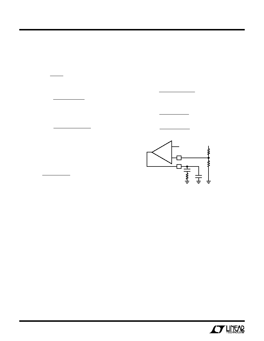
3425p
Linear Technology Corporation
1630 McCarthy Blvd., Milpitas, CA 95035-7417
(408) 432-1900
q
FAX: (408) 434-0507
q
www.linear.com
©
LINEAR TECHNOLOGY CORPORATION 2003
LT/TP 0603 1K PRINTED IN USA
TYPICAL APPLICATIO
U
10MHz, High Current, Very Low Profile, 8-Phase Converter Using Two LTC3425s Operating
in Fixed Frequency Mode with Forced CCM (Max Component Height = 1.6mm)
L5
1
µ
H
C
IN2
2.2
µ
F
R6
75k
R
T2
14.7k
R
F4
17.4k
R
F3
10.2k
L6
1
µ
H
L7
1
µ
H
L8
1
µ
H
C
IN1,2
: TAIYO YUDEN JMK107BJ225MA
C
OUT
: TAIYO YUDEN JMK212BJ475MG (
×
8)
L1 TO L8: MURATA LQH32CN1R0M51
V
IN
SWA
SWB
LTC3425
SWC
SWD
SGND
SHDN
V
OUTS
V
OUTA
V
OUTB
V
OUTC
V
OUTD
REFOUT
CCM
REFEN
SYNCIN
BURST
R
T
I
LIM
PGOOD
SYNCOUT
SS
FB
COMP
GNDA
GNDB
GNDC
GNDD
C1
330pF
3425 TA05
C
OUT2
4.7
µ
F
×
4
C
SS
0.022
µ
F
R3
33k
R
F2
17.4k
R4
100k
PGOOD
R
F1
10.2k
V
OUT
3.3V
5A
L1
1
µ
H
C
IN1
2.2
µ
F
R5
75k
R
T1
12.1k
L2
1
µ
H
L3
1
µ
H
L4
1
µ
H
V
IN
V
OUT
V
IN
2.5V
SWA
SWB
LTC3425
SWC
SWD
SGND
SHDN
V
OUTS
V
OUTA
V
OUTB
V
OUTC
V
OUTD
REFOUT
CCM
REFEN
SYNCIN
BURST
R
T
I
LIM
PGOOD
SYNCOUT
SS
FB
COMP
GNDA
GNDB
GNDC
GNDD
C
OUT1
4.7
µ
F
×
4
V
OUT
RELATED PARTS
PART NUMBER
DESCRIPTION
COMMENTS
LT
®
1370/LT1370HV
6A (I
SW
) 500kHz, High Efficiency Step-Up DC/DC
V
IN
: 2.7V to 30V, V
OUT(MAX)
: 35V/42V, I
Q
: 4.5mA, I
SD
: <12
µ
A,
Converters
DD, TO220-7
LT1371/LT1371HV
3A (I
SW
) 500kHz, High Efficiency Step-Up DC/DC
V
IN
: 2.7V to 30V, V
OUT(MAX)
: 35V/42V, I
Q
: 4mA, I
SD
: <12
µ
A,
Converters
DD, TO220-7, S20
LT1613
550mA (I
SW
) 1.4MHz, High Efficiency Step-Up DC/DC
90% Efficiency, V
IN
: 0.9V to 10V, V
OUT(MAX)
: 34V, I
Q
: 3mA,
Converter
I
SD
: <1
µ
A, ThinSOT
LT1618
1.5A (I
SW
) 1.25MHz, High Efficiency Step-Up DC/DC
90% Efficiency, V
IN
: 1.6V to 18V, V
OUT(MAX)
: 35V, I
Q
: 1.8mA,
Converter
I
SD
: <1
µ
A, MS10
LTC1700
No R
SENSE
TM
530kHz, Synchronous Step-Up
95% Efficiency, V
IN
: 0.9V to 5V, I
Q
: 200
µ
A, I
SD
: <10
µ
A, MS10
DC/DC Controller
LTC1871
Wide Input Range, 1MHz, No R
SENSE
Current Mode Boost, 92% Efficiency, V
IN
: 2.5V to 36V, I
Q
: 250
µ
A, I
SD
: <10
µ
A, MS10
Flyback and SEPIC Controller
LT1930/LT1930A
1A (I
SW
) 1.2MHz/2.2MHz, High Efficiency Step-Up DC/DC
High Efficiency, V
IN
: 2.6V to 16V, V
OUT(MAX)
: 34V, I
Q
: 4.2mA/5.5mA,
Converters
I
SD
: <1
µ
A, ThinSOT
LT1946/LT1946A
1.5A (I
SW
) 1.2MHz/2.7MHz, High Efficiency Step-Up
High Efficiency, V
IN
: 2.45V to 16V, V
OUT(MAX)
: 34V, I
Q
: 3.2mA,
DC/DC Converters
I
SD
: <1
µ
A, MS8
LT1961
1.5A (I
SW
) 1.25MHz, High Efficiency Step-Up DC/DC
90% Efficiency, V
IN
: 3V to 25V, V
OUT(MAX)
: 35V, I
Q
: 0.9mA,
Converter
I
SD
: 6
µ
A, MS8E
LTC3400/LTC3400B
600mA (I
SW
) 1.2MHz, Synchronous Step-Down DC/DC
92% Efficiency, V
IN
: 0.85V to 5V, V
OUT(MAX)
: 5V, I
Q
: 19
µ
A/300
µ
A,
Converters
I
SD
: <1
µ
A, ThinSOT
LTC3401
1A (I
SW
) 3MHz, Synchronous Step-Up DC/DC Converter
97% Efficiency, V
IN
: 0.5V to 5V, V
OUT(MAX)
: 6V, I
Q
: 38
µ
A, I
SD
: <1
µ
A,
MS10
LTC3701
2-Phase, 550kHz, Low Input Voltage, Dual Step-Down
97% Efficiency, V
IN
: 2.5V to 10V, I
Q
: 460
µ
A, I
SD
: <9
µ
A, SSOP-16
DC/DC Controller