Äîêóìåíòàöèÿ è îïèñàíèÿ www.docs.chipfind.ru
FUJITSU SEMICONDUCTOR
DATA SHEET
8-bit Proprietary Microcontroller
CMOS
F
2
MC-8L MB89980 Series
MB89983/P985/PV980
s
DESCRIPTION
The MB89980 series is a line of the general-purpose, single-chip microcontrollers. In addition to a compact
instruction set, the microcontrollers contain a variety of peripheral functions such as an LCD controller/driver,
an A/D converter, timers, remote control transmission output, buzzer output, PWM timers, and external interrupts.
s
FEATURES
· F
2
MC-8L family CPU core
· Dual-clock control system
· Maximum memory size: 8-Kbyte ROM, 256-byte RAM (max.)
· Minimum execution time: 0.95
µ
s/4.2 MHz
· I/O ports: max. 47 channels (max. 13 high-current type)
· 21-bit time-base counter
· 8/16-bit timer/counter: 8bit x 2 channels or 16-bit x 1 channels
· External interrupts (wake-up function): Four channels with edge selection plus eight level-interrupt channels
· 8-bit A/D converter: 4 channels
· 8-bit PWM timers: 2 channels
· Watch prescaler (15 bits)
· LCD controller/driver: 14 segments
×
4 commons (max. 56 pixels)
· LCD driving reference voltage generator
· Remote control transmission output
· Buzzer output
· Power-on reset function (option)
· Low-power consumption modes (stop, sleep, and watch mode)
· CMOS technology
s
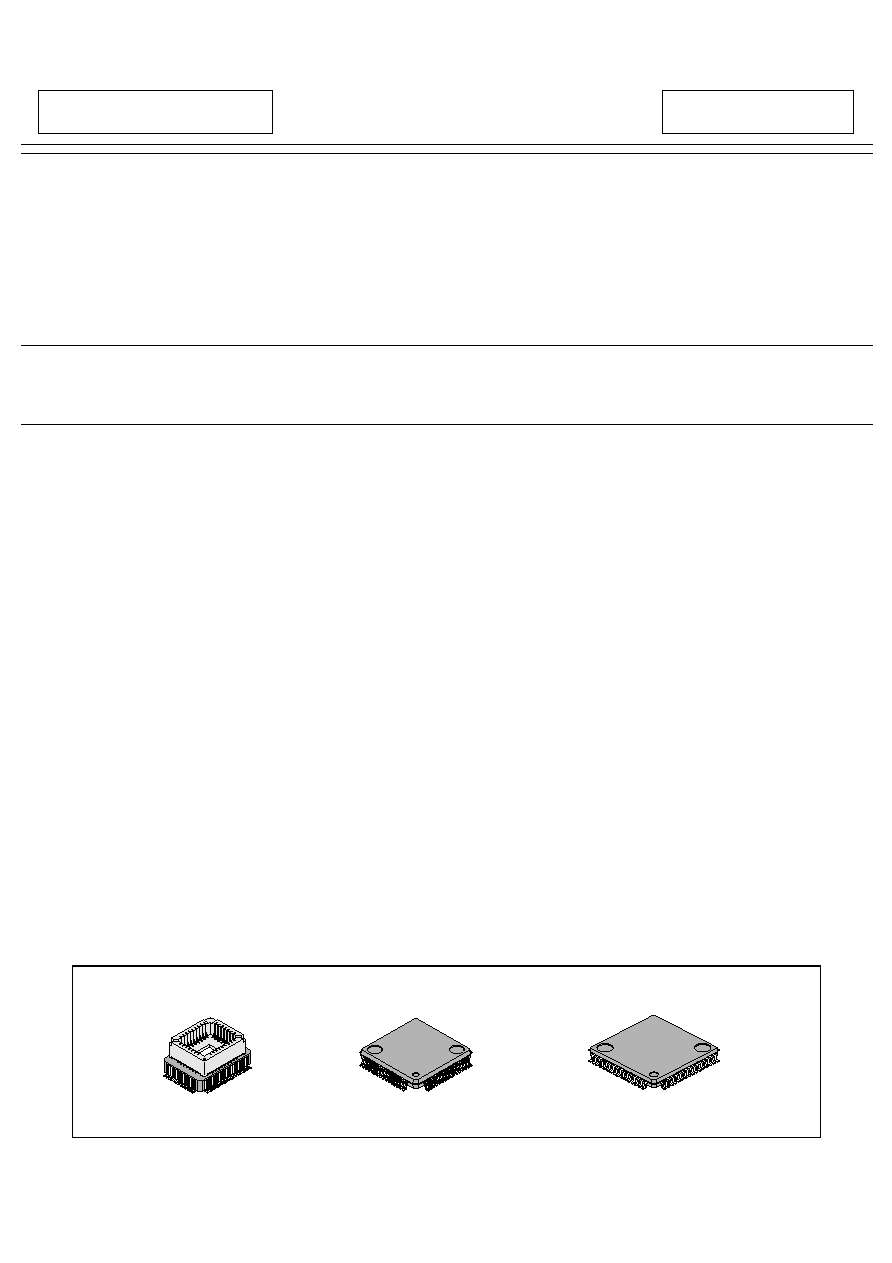
PACKAGE
(FPT-64P-M03)
(FPT-64P-M09)
(FPT-64P-M09)
64-pin Plastic QFP
(FPT-64P-M03)
64-pin Plastic LQFP
(MQP-64C-P01)
64-pin Ceramic MQFP
(MQP-64C-P01)
Revision 3.0
2
MB89980 Series
s
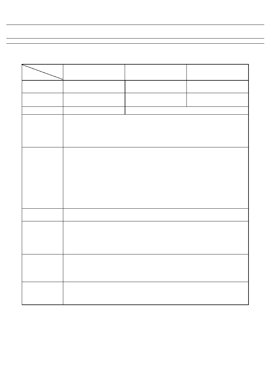
PRODUCT LINEUP
(Continued)
MB89983
MB89P985
MB89PV980
Classification
Mass production products
(mask ROM products)
One-time PROM product (OTP)
Piggyback/evaluation
product (for development)
ROM size
8 K x 8 bits
(internal mask ROM)
16K x 8 bits
(Internal PROM)
32K x 8 bits
(External ROM)
RAM size
256
×
8 bits
512 x 8 bits
CPU functions
Number of instructions:
136
Instruction bit length:
8 bits
Instruction length:
1 to 3 bytes
Data bit length:
1, 8,16 bits
Minimum execution time:
0.95
µ
s/4.2 MHz
Interrupt processing time:
9
µ
s/4.2 MHz
Ports
General-purpose I/O ports (N-ch open-drain):
8 (4 ports also serve as peripherals,
3 ports are heavy-current drive type.)
Output-only ports (N-ch open-drain):
20 (4 ports also serve as A/D, 14 ports
serve as segment pins and 2 ports serve
as common pins, 10 ports are heavy-
current drive type .)
General-purpose I/O ports (CMOS): 16 (12 ports also serve as an external
interrupt, )
Input-only ports (CMOS) 2 (serve with sub-clock pins)
Output-only ports (CMOS) 1 (serves as peripherials
Total:
47 (max.)
Timer/counter
8-bit timer operation (toggled output capable, operating clock cycle 1.9
µ
s to 486
µ
s)
16-bit timer operation (toggled output capable, operating clock cycle 1.9
µ
s to 486
µ
s)
LCD controller/driver
Common output:
4 (max.)
Segment output:
14 (max.)
*2
Bias power supply pins:
4
LCD display RAM size:
14
×
4 bits
Dividing resistor for LCD driving:
Built-in (an external resistor
selectability)
A/D converter
8-bit resolution
×
4 channels
A/D conversion mode (conversion time 43
µ
s/4.2 MHz (44 instruction cycles))
Sense mode (conversion time 11.9
µ
s/4.2 MHz)
Continuous activation by an internal timer capable
Reference voltage input
PWM timer 1,
PWM timer 2
8 bits
×
2 channels
8-bit reload timer operation (toggled output capable, operating clock cycle: 0.95
µ
s to 124
ms)
8-bit resolution PWM operation (conversion cycle: 243
µ
s to 32 s)
Part number
Parameter
3
MB89980 Series
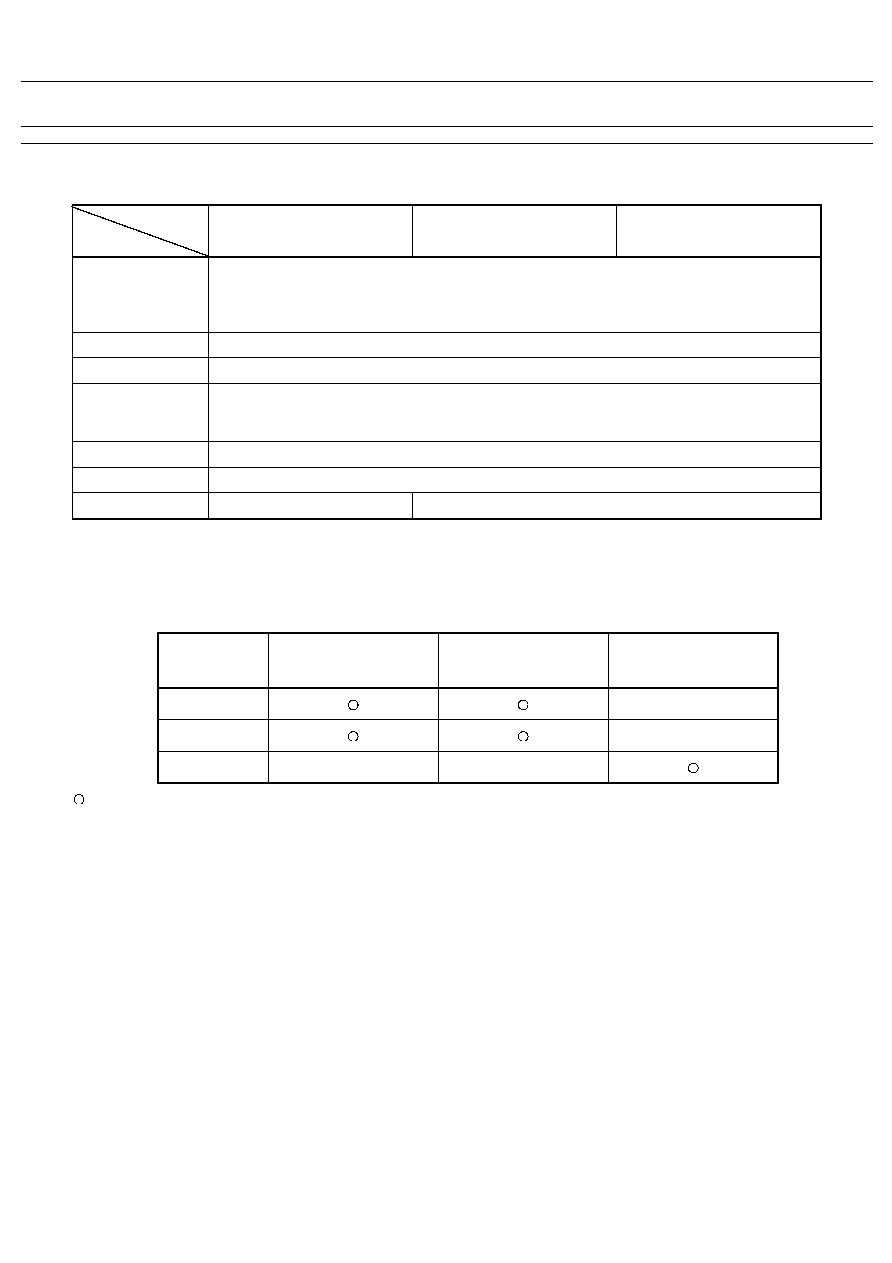
(Continued)
*1: Varies with conditions such as the operating frequency. (The operating voltage of the A/D converter is assured
separately. See section "
s
Electrical Characteristics.")
*2: See section "
s
Mask Options."
s
PACKAGE AND CORRESPONDING PRODUCTS
: Available
×
: Not available
Note: For more information about each package, see section "
s
Package Dimensions."
MB89983
MB89P985
MB89PV980
External interrupt 1
(wake-up function)
4 independent channels (edge selectability)
Rising edge/falling edge selectability
Used also for wake-up from stop/sleep mode.
(Edge detection is also permitted in stop mode.)
External interrupt 2
"L" level interrupts
×
8 channels
Buzzer output
1 (7 frequencies are selectable by the software.)
Remote control
transmission
output
1 (Pulse width and cycle are software selectable.)
Standby modes
Subclock mode, sleep mode, stop mode, and watch mode
Process CMOS
Operating voltage
*1
2.2 V to 6.0 V
2.7 V to 6.0 V
Package MB89983
MB89P985
MB89PV980
FPT-64P-M09
×
FPT-64P-M03
×
MQP-64C-P01
×
×
Part number
Parameter

4
MB89980 Series
s
DIFFERENCES AMONG PRODUCTS
1. Memory Size
Before evaluating using the piggyback product, verify its differences from the product that will actually be used.
Take particular care on the following points:
· The stack area, etc., is set at the upper limit of the RAM.
2. Current Consumption
· In the case of the MB89PV980, add the current consumed by the EPROM which is connected to the top socket.
· When operated at low speed, the product with an OTPROM (one-time PROM) or an EPROM will consume
more current than the product with a mask ROM.
However, the current consumption in the sleep/stop modes is the same. (For more information, see section
"
s
Electrical Characteristics.")
3. Mask Options
Functions that can be selected as options and how to designate these options vary by the product.
Before using options check section "
s
Mask Options."
Take particular care on the following points:
· A pull-up resistor is not selectable for P40 to P47 and P60 to P65 if they are used as LCD pins.
· A pull-up resistor is not selectable for P50 to P53 if they are used as analog input.
4. Pull-up resistor
Pull-up resisitors of MB89P985 and MB89PV980 are selected by pull-up control registor (Port 0, 1, 5), but there
are no pull-up resistor for Port 2, 4 and 6 in MB89P985 and MB89PV980.
ALL pull-up resistor of MB89983 are selected by mask option (Port 0, 1, 2, 4, 5, 6)
5. Segment/Common port
The Segment/Port , Common/Port output in MB89P985 and MB89PV980 are selected by control register, LCR2.
The Segment/Port , Common/Port output in MB89983 are selected by mask option.
5
MB89980 Series
s
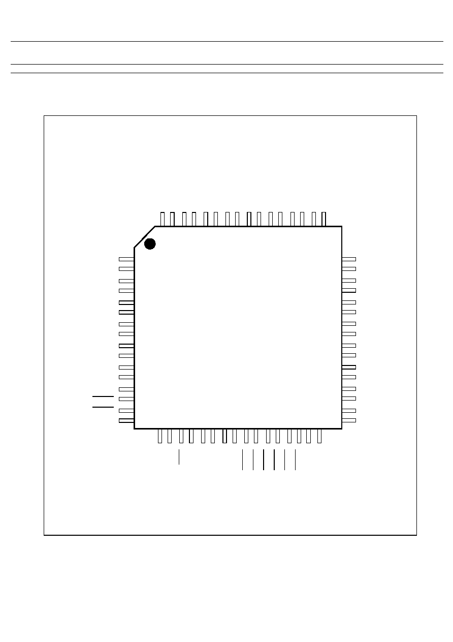
PIN ASSIGNMENT
V1
V0
P27/PWM2*
1
P26*
1
P25
P24/RCO
P23
P22/TO
P21*
1
P20/EC
P17
P16
P15
P14
P13/INT13
P12/INT12
P47
/
SE
G
7
*
1
*
4
P46
/
SE
G
6
*
1
*
4
P45
/
SE
G
5
*
1
*
4
P44
/
SE
G
4
*
1
*
4
P43
/
SE
G
3
*
1
*
5
P42
/
SE
G
2
*
1
*
5
P41
/
SE
G
1
*
1
*
5
P40
/
SE
G
0
*
1
*
5
Vc
c
P71
/
CO
M3
*
3
P70
/
CO
M2
*
3
COM1
COM0
V3
V2
Vs
s
P3
1/X
0
A*
2
P3
2/X
1
A*
2
RS
T
MO
D0
MO
D1
X0
X1
Vs
s
P02
/INT22
P03
/INT23
P04
/INT24
P05
/INT25
P06
/INT26
P07
/INT27
P10
/INT10
P11
/INT11
P60/SEG8*
1
*
3
P61/SEG9*
1
*
3
P62/SEG10*
6
P63/SEG11*
6
P64/SEG12*
6
P65/SEG13*
6
P50/AN0
P51/AN1
P52/AN2
P53/AN3
AVcc
AV
R
AVss
P00/INT20
P01/INT21
P30/PWM1/BZ
48
47
46
45
44
43
42
41
40
39
38
37
36
35
34
33
64
63
62
61
60
59
58
57
56
55
54
53
52
51
50
49
17
18
19
20
21
22
23
24
25
26
27
28
29
30
31
32
1
2
3
4
5
6
7
8
9
10
11
12
13
14
15
16
TOP VIEW
QFP-64
(FPT-64P-M09)
(FPT-64P-M03)
*1: Heavy-current drive type
*2: When the dual clock system is selected
*3, *4, *5, *6: Selected using mask option in MB89983, but selected by software in MB89P985 and MB89PV980.
Document Outline