EXAR Corporation, 48720 Kato Road, Fremont, CA 94538
·
(510) 668-7000
·
FAX (510) 668-7017
Rev. P2.00
Preliminary
XRD64L42
Dual 10-Bit 40MSPS CMOS ADC
October 2000-2
FEATURES
·
10-Bit Resolution
·
Two Monolithic Complete 10-Bit ADCs
·
40 MSPS Conversion Rate
·
On-Chip Track-and-Hold
·
On-Chip Voltage Reference
·
Low 5 pF Input Capacitance
·
TTL/CMOS Outputs
·
Tri-State Output Buffers
·
Single +3.0V Power Supply Operation
·
Low Power Dissipation: 200mW-typ @ 2.7V
·
Power Down Mode Less Than 5mW
·
-40°C to +85°C Operation Temperature Range
APPLICATIONS
·
Medical Ultrasound Imaging
·
I & Q Modems
BENEFITS
·
Reduction of Components
·
Reduction of System Cost
·
High Performance @ Low Power Dissipation
·
Long Term Time and Temperature Stability
GENERAL DESCRIPTION
The XRD64L42 is two 10-bit, monolithic, 40 MSPS
ADCs. Manufactured using a standard CMOS pro-
cess, the XRD64L42 offers low power, low cost and
excellent performance. The on-chip track-and-hold
amplifier(T/H) and voltage reference (VREF) eliminate
the need for external active components, requiring only
an external ADC conversion clock for the application.
The XRD64L42 analog input can be driven with ease
due to the high input impedance of RIN = 25KOhms
and CIN = 5pF.
The design architecture uses 17 time- interleaved 10-
bit SAR ADCs in each converter to achieve high
conversion rate of 40 MSPS minimum. In order to
insure and maintain accurate 10-bit operation with
respect to time and temperature, XRD64L42 incorpo-
rates an auto-calibration circuit which continuously
adjusts and matches the offset and linearity of each
ADC. This auto-calibration circuit is transparent to the
user after the initial 3.4ms calibration (168,000 initial
clock cycles).
The power dissipation is only 200mW at 40 MSPS with
+2.7V power supply.
The digital output data is straight binary format, and
the tri-state disable function is provided for common
bus interface.
The XRD64L42 internal reference provides cost sav-
ings and simplifies the design/development. The out-
put voltage of the internal reference is set by two
external resistors. The internal reference can be dis-
abled if an external reference is used for a power
savings of 50mW.
ORDERING INFORMATION
Part Number
Package Type
Temperature Range
XRD64L42AIV
64-Lead TQFP
-40°C to +85°C

XRD64L42
2
Rev. P2.00
Preliminary
Figure 1. XRD64L42 Simplified Block Diagram
DB9 - DB0,
OTRB
DA9 - DA0,
OTRA
CONTROL LOGIC
Bandgap
+
-
V B G
VFBK
VRHF
VRLF
VINB+ VINB-
TRI_B
A/D 1b
A/D 17b
ADC B
10 Bit A/D's
11
ADC A
A/D 1a
A/D 17a
10 Bit A/D's
11
CLAMP
SYNCO
TRI_A
VINA+ VINA-
K
PD
CKIN
DIFF
VCLMPA
VCLMPB
+
-
VCMO
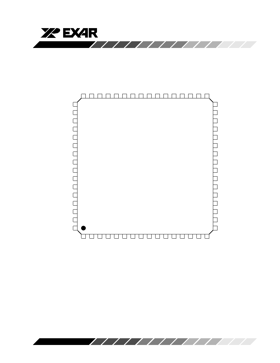
XRD64L42
3
Rev. P2.00
Preliminary
VBG
VFBK
VRHF
VRHF
VRLF
VRLF
1
2
3
4
5
6
7
8
9
1 0
1 1
1 2
1 3
1 4
1 5
1 6
17
18
19
20
21
22
23
24
25
26
27
28
29
30
31
32
3 3
3 4
3 5
3 6
3 7
3 8
3 9
4 0
4 1
4 2
4 3
4 4
4 5
4 6
4 7
4 8
49
50
52
51
53
54
55
56
57
58
59
60
61
62
63
64
VCLMPA
DGND
DGND
PD
DVDD
TRI_B
DIFF
CLAMP
T R I _ A
C K I N
S Y N C O
D B 0
D B 1
D B 2
D O G N D
D O V D D
D G N D
D B 4
D B 9
D B 8
D B 7
D B 5
D B 6
D B 3
OTRB
DA0
DA1
DA2
DA3
DA4
DOVDD
DOGND
DVDD
DGND
DA5
DA6
DA7
DA8
DA9
OTRA
V C M O
D G N D
A G N D
A V D D
A G N D
A G N D
VINB-
V I N B +
A G N D
V I N A +
VINA-
A G N D
A V D D
A V D D
A G N D
A G N D
XRD64L42 64QFP
VCLMPB
AGND

XRD64L42
4
Rev. P2.00
Preliminary
PIN DESCRIPTION
Pin #
Symbol
Description
1
VBG
Bandgap Voltage Output
2
VFBK
Analog Reference Feedback
3
VRHF
Top Voltage Reference Force
4
VRHF
Top Voltage Reference Force
5
VRLF
Bottom Voltage Reference Force
6
VRLF
Bottom Voltage Reference Force
7
VCLMPA
Analog Input Clamp A
8
VCLMPB
Analog Input Clamp B
9
AGND
Analog Ground
10
DGND
Digital Ground
11
DGND
Digital Ground
12
PD
Power Down
13
DVDD
Digital Supply Voltage
14
TRI_B
Tri-state for the B Channel Outputs
15
DIFF
Differential / Single-Ended Input Mode
16
CLAMP
Digital Clamp Control
17
TRI_A
Tri-state for the A Channel Outputs
18
CKIN
Clock Input
19
SYNCO
Data Valid Output
20
DB0
Digital Output Bit 0 (LSB) ADC B
21
DB1
Digital Output Bit 1 ADC B
22
DB2
Digital Output Bit 2 ADC B
23
DOGND
Digital Output Ground
24
DOVDD
Digital Output Supply Voltage
25
DGND
Digital Ground
26
DB3
Digital Output Bit 3 ADC B
27
DB4
Digital Output Bit 4 ADC B
28
DB5
Digital Output Bit 5 ADC B
29
DB6
Digital Output Bit 6 ADC B
30
DB7
Digital Output Bit 7 ADC B
31
DB8
Digital Output Bit 8 ADC B
32
DB9
Digital Output Bit 9 (MSB) ADC B
33
OTRB
Over Range Digital Output Bit ADC B
34
DA0
Digital Output Bit 0 (LSB) ADC A
35
DA1
Digital Output Bit 1 ADC A
36
DA2
Digital Output Bit 2 ADC A
37
DA3
Digital Output Bit 3 ADC A
38
DA4
Digital Output Bit 4 ADC A
39
DOVDD
Digital Output Supply Voltage
40
DOGND
Digital Output Ground
41
DVDD
Digital Supply Voltage

XRD64L42
5
Rev. P2.00
Preliminary
Pin #
Symbol
Description
42
DGND
Digital Ground
43
DA5
Digital Output Bit 5 ADC A
44
DA6
Digital Output Bit 6 ADC A
45
DA7
Digital Output Bit 7 ADC A
46
DA8
Digital Output Bit 8 ADC A
47
DA9
Digital Output Bit 9 ADC A
48
OTRA
Over Range Digital Output Bit ADC A
49
VCMO
Differential Common Mode Voltage Output
50
DGND
Digital Ground
51
AGND
Analog Ground
52
AVDD
Analog Supply Voltage
53
AGND
Analog Ground
54
AGND
Analog Ground
55
VINB-
Analog Input B(-)
56
VINB+
Analog Input B(+)
57
AGND
Analog Ground
58
VINA+
Analog Input A(+)
59
VINA-
Analog Input A(-)
60
AGND
Analog Ground
61
AVDD
Analog Supply Voltage
62
AVDD
Analog Supply Voltage
63
AGND
Analog Ground
64
AGND
Analog Ground
PIN DESCRIPTION (CONT'D)