© P
ROGRAMMABLE
S
ILICON
S
OLUTIONS
, 2002
DS007 V1.3 2/03
P
ROGRAMMABLE
S
ILICON
S
OLUTIONS
P
R
E
L
IM
IN
A
R
Y
Characteristics subject to change without notice
PS01TR01
IEEE 802.11B(G) Compliant
2.4GHz WLAN Transceiver
FEATURES
· IEEE 802.11B Compliant
Supports CCK/DSSS Modes
1, 2, 5.5, 11Mbps (CCK / DSSSS / PBCC)
6, 9, 12, 18, 24, 36, 48, 54Mbps (OFDM)
· High Level of Integration
Integrated VCO / Synthesizer
Integrated LNA
Integrated Power Amplifier
SuperHeterodyne Architecture
Single Chip With External SAW Filter
All CMOS Implementation
· Receiver Sensitivity
CCK: -82dBm
DSSS: -90dBm
· Transmitter Power
+22dBm @ P1dB
· Available Package
48-Pin QFN (7mm x 7mm)
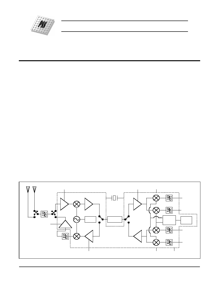
PRODUCT DESCRIPTION
The PS01TR01 is a highly integrated CMOS single
transceiver chip solution for 802.11B(G) WLAN appli-
cations. The transceiver is fully compliant with IEEE
802.11B(G) standards. It supports both PFDM and
CCK/DSSS/PBCC mode.
The chip is a high performance and low DC power
consumption SuperHeterodyne architecture. It
requires only one external SAW filter for channel filter-
ing. The transceiver does not require RF balun for the
receive input and transmit output. The baseband IQ
input and output are differential and DC coupled. The
receiver provides 100dB AGC range -30dB in the LNA
and 70dB in the IF amplifier. The transceiver has
power saving mode build-in. At 3.3V power supply, the
radio power consumption during receive mode is typi-
cally 51mA and 53mA in transmit mode. THe power
amplifier draws typically 250mA. The low receive
power consumption makes this chip ideal for portable
wireless applications such as PDA, cellular phone, and
laptop computers.
The chip comes in a 48-pin QFN.
CHIP BLOCK DIAGRAM
SAW
90
o
0
o
RXI
RXQ
TXI
TXQ
PLL
AGC
ANT#1
ANT#2
RX AGC
PLL
AGC
DET
TX AGC
H/L Gain
44MHz
XTAL
RSSI
PWR CTL
SPI
PS01TR01
PS01TR01
2
OF
13
WWW
.
PS
2
TECH
.
COM
P
R
E
LI
M
IN
A
R
Y
Characteristics subject to change without notice
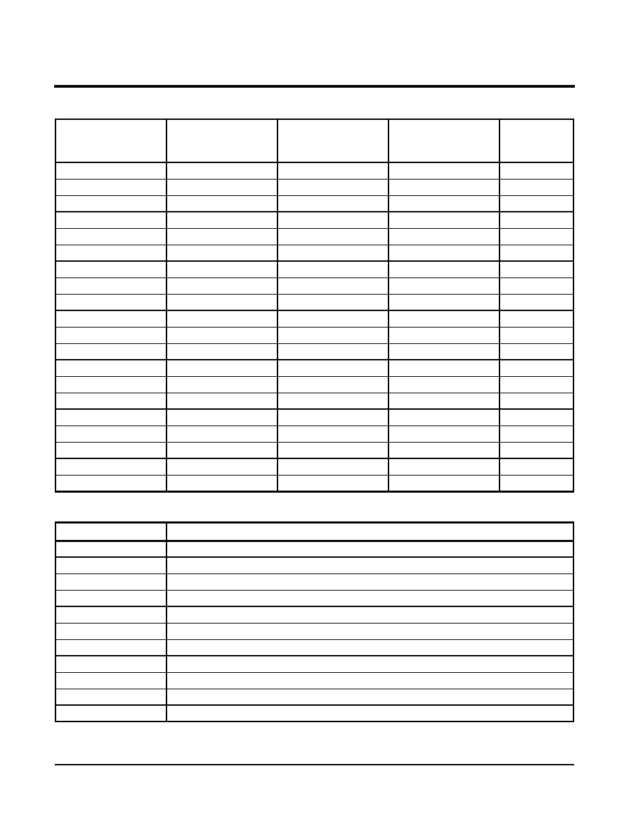
PIN ASSIGNMENT AND DESCRIPTION
Pin
Function
Description
Interface
1
TX_UPC_VDD
Transmit upconverter positive power supply
2.7V~3.6V
2
TA_FLT_OUT
Transmit upconverter output to image filter
50
output
3
LNA_VDD
Receiver low noise amplifier positive power supply
2.7V~3.6V
4
GND
Ground
5
RFIN
Receiver low noise amplifier input
50
output
6
GND
Ground
7
TX_FLT_IN
Transmit power amplifier input from image filter
50
output
8
RFAGC_CTL
Receiver low noise amplifier High/Low gain select input
CMOS logic input
9
TX_RFA_VDD
Transmit pre-amplifier positive power supply
2.7V~3.6V
10
TX_PA_PD
Transmit power amplifier power down control
Shunt capacitor
11
TX_PA_VDD1
Transmit power amplifier positive power supply, 1
st
stage
2.7V~3.6V
12
TX_PA_DET
transmit power detector output
1.5V to 2V
13
TX_PA_OUT
Transmit power amplifier output
50
output
14
TX_PA_VDD2
transmit power amplifier positive power supply
2.7V~3.6V
15
REF_IN
44MHz reference clock in or 44MHz crystal
CMOS logic input
16
REF_OUT
44MHz reference clock out or 44MHz crystal
CMOS logic output
17
RF_PLL_VDD
RF phase locked loop digital positive power supply
2.7V~3.6V
18
TX_IP
Baseband in-phase transmit positive input
1.2V input com. mode
19
TX_IN
Baseband in-phase transmit negative input
1.2V input com. mode
20
TX_QN
Baseband quadrature-phase transmit negative input
1.2V input com. mode
21
TX_QP
Baseband quadrature-phase transmit positive input
1.2V input com. mode
22
TX_LPF_VDD
Baseband transmit low pass filter positive power supply
2.7V~3.6V
23
IF_PLL_VDD
IF phase locked loop positive power supply
2.7V~3.6V
24
TX_IF_VDD2
Baseband IF transmit amplifier positive power supply
2.7V~3.6V
25
BB_IFP
Baseband IF positive input/output from/to SAW filter
900
differential
26
BB_IFN
Baseband IF negative input/output from/to SAW filter
900
differential
27
RX_AGC_VDD1
RX IF AGC amplifier (1) positive power supply
2.7V~3.6V
28
RX_VAGC
RX IF AGC amplifier gain control input
0.8V~2.2V
29
RX_AGC_VDD2
RX IF AGC amplifier (2) and demodulator positive power
supply
2.7V~3.6V
30
LD
RF and IF synthesizers' lock detect output
CMOS logic output
31
RX_IP
Baseband in-phase receive positive output
1.2/1.7V output com.
mode
32
RX_IN
Baseband in-phase receive negative output
1.2/1.7V output com.
mode
33
TX_QP
Baseband quadrature-phase receive positive output
1.2/1.7V output com.
mode
PS01TR01
3
OF
13
DS007 V1.3 2/03
Programmable Silicon Solutions
P
R
E
L
IM
IN
A
R
Y
Characteristics subject to change without notice
BASEBAND INTERFACE SPECIFICATIONS
Pin
Function
Description
Interface
34
RX_QN
Baseband quadrature-phase receive negative output
1.2/1.7V output com.
mode
35
PE1
Radio power control logic input (1)
CMOS logic input
36
PE2
Radio power control logic input (2)
CMOS logic input
37
RX_LPF_VDD
Baseband receive low pass filter positive power supply
2.7V~3.6V
38
CMREF
Common reference voltage for baseband receive output
1.2/1.7V
39
LE
Latch enable input for radio register programming
CMOS logic input
40
CLK
Clock input for radio register programming
CMOS logic input
41
Data
Data input for radio register programming
CMOS logic input
42
RF_CP_DO
RF phase locked loop charge pump output
0.5V~2.5V
43
RF_VCO_VDD
RF phase locked loop VCO positive power supply
2.7V~3.6V
44
RF_VCO_TUNE
RF phase locked loop VCO frequency tuning input
0.5V~2.5V
45
RF_IFN
RF IF negative input/output from/to SAW filter
800
differential
46
RF_IFP
RF IF positive input/output from/to SAW filter
800
differential
47
RF_IF_VDD
RF transmit and receive IF amplifier positive power supply
2.7V~3.6V
48
TX_IF_AGC
TX IF AGC amplifier gain control input
0.8V~2.2V
Pin
Function
Description
Interface
8
RFAGC_CTL
Min. High = Vdd-0.2V
Max. Low = 0.2V
Settling Time: 100ns
Input Impedance = 1M
|| 5pF
10
TX_PA_PD
Internal 4K
+ external shunt capacitor set power
ramp up and ramp down timing
68pF
12
TX_PA_DET
Min. output = 1.5V
Max. output = 2.2V
Slope = Positive
Settling Time = 10
µ
S
Load Impedance = 15pF
16
REF_OUT
Min. High = Vdd-0.2V
Max. Low = 0.2V
44MHz output
Ouput Load: 15pF
18
TX_IP
1.2+0.1V common mode input
50+25mVp signal input
Max. differential offset = 5mV
Input Impedance = 1M
|| 5pF
19
TX_IN
1.2+0.1V common mode input
50+25mVp signal input
Max. differential offset = 5mV
Input Impedance = 1M
|| 5pF
20
TX_QP
1.2+0.1V common mode input
50+25mVp signal input
Max. differential offset = 5mV
Input Impedance = 1M
|| 5pF
21
TX_QN
1.2+0.1V common mode input
50+25mVp signal input
Max. differential offset = 5mV
Input Impedance = 1M
|| 5pF
28
RX_VAGC
Min. input = 0.5V
Max. input = 2.2V
Gain range = -5dB to 75dB
Slope = Negative
Max. TX/RX settling time = 500ns
Max. VAGC settling time = 300ns
Input Impedance = 1M
|| 5pF
PS01TR01
4
OF
13
WWW
.
PS
2
TECH
.
COM
P
R
E
LI
M
IN
A
R
Y
Characteristics subject to change without notice
PS01TR01 POWER CONTROL INTERFACE SPECIFICATIONS
Pin
Function
Description
Interface
30
LD
Min. High = Vdd-0.2V
Max. Low = 0.2V
Lock = High
Load Inpedance = 15pF
31
RX_IP
1.2(1.7)+0.1V common mode output
500+250mVp signal output
Max. differential offset = 20mV
Load Impedance = 10pF
32
RX_IN
1.2(1.7)+0.1V common mode output
500+250mVp signal output
Max. differential offset = 20mV
Load Impedance = 10pF
33
RX_QP
1.2(1.7)+0.1V common mode output
500+250mVp signal output
Max. differential offset = 20mV
Load Impedance = 10pF
34
RX_QN
1.2(1.7)+0.1V common mode output
500+250mVp signal output
Max. differential offset = 20mV
Load Impedance = 10pF
35
PE1
Min. High = Vdd-0.2V
Max. Low = 0.2V
See power enable table
Input Impedance = 1M
|| 5pF
36
PE2
Min. High = Vdd-0.2V
Max. Low = 0.2V
See power enable table
Input Impedance = 1M
|| 5pF
38
CMREF
Mode1 = 1.2+0.1V
Mode2 = 1.7+0.1V
Mode1 and Mode1 selectable
through a register
Input Impedance = 1M
|| 15pF
39
LE
Min. High = Vdd-0.2V
Max. Low = 0.2V
CMOS logic input
Input Impedance = 1M
|| 5pF
40
CLK
Min. High = Vdd-0.2V
Max. Low = 0.2V
CMOS logic input
Input Impedance = 1M
|| 5pF
41
DATA
Min. High = Vdd-0.2V
Max. Low = 0.2V
CMOS logic input
Input Impedance = 1M
|| 5pF
48
TX_IF_AGC
Min. input = 0.5V
Max. input = 2.2V
Gain range = 0dB to 30dB
Slope = Negative
Max. TX/RX settling time = 500ns
Max. VAGC settling time = 300ns
Input Impedance = 1M
|| 5pF
PE1
PE2
M(2) (PLL_PE)
(Serial Bus)
Interface
0
0
1
Power Down State, PLL Registers in Save Mode, Inactive PLL,
Active Serial Interface
0
1
1
Receive State, Active PLL. Receive ready in 2
µ
S
1
0
1
Transmit State, Active PLL. Receive ready in 2
µ
S
1
1
1
Inactive Transmit and Receive States, Active PLL, Active Serial
Interface
X
X
0
Power Down State, Inactive PLL, Active Serial Interface
PS01TR01
5
OF
13
DS007 V1.3 2/03
Programmable Silicon Solutions
P
R
E
L
IM
IN
A
R
Y
Characteristics subject to change without notice
PS01TR01 REGISTER MAP
PS01TR01 REGISTER DEFINITIONS
PLLs Programming
PLLs Programming
+ Operational Mode
Receive Offset Cali-
bration + Operation-
al Mode
Transmit Offset Cal-
ibration + Filter BW
Selection
Serial Bits
0
0
1
1
LSB1
0
1
0
1
2
A(0)
RR(6)
CR(0)
CT(0)
3
A(1)
IN(0)
CR(1)
CT(1)
4
A(2)
IN(1)
CR(2)
CT(2)
5
A(3)
IN(2)
CR(3)
C4(3)
6
A(4)
IN(3)
CR(4)
CT(4)
7
B(0)
IN(4)
CR(5)
CT(5)
8
B(1)
IN(5)
CR(6)
CT(6)
9
B(2)
IR(0)
CR(7)
CT(7)
10
B(3)
IR(1)
X
X
11
B(4)
IR(2)
X
X
12
B(5)
IR(3)
X
X
13
B(6)
M(0)
X
X
14
RR(0)
M(1)
R(0)
T(0)
15
RR(1)
M(2)
R(1)
T(1)
16
RR(2)
DCT
R(2)
T(2)
17
RR(3)
DCR
R(3)
T(3)
18
RR(4)
DEF
X
X
19
RR(5)
IFT
X
X
MSB
Bits
Description
A(0-4)
5-Bit RF PLL A-Counter
B(0-6)
7-Bit RF PLL B-Counter
RR(0-6)
7-Bit RF PLL Reference Counter
IN(0-5)
6-Bit IF PLL N-Counter
IR(0-3)
4-Bit IF PLL reference Counter
CR(0-7)
8-Bit Baseband Receive IQ Output DC Offset Cancellation Adjustment
CT(0-7)
8-Bit Baseband Transmit IQ Output DC Offset cancellation Adjustment
T(0-3)
4-Bit Transmit Filter Bandwidth Control. Range = 7 to 14MHz 3dB Bandwidth
R(0-3)
4-Bit Receive Filter Bandwidth Control. Range = 7 to 14MHz 3dB Bandwidth
DCR
Receive Output Common Mode DC Selection (0 = 1.2V or 1 = 1.7V)
DCT
Transmit Output Common Mode DC Selection (0 = 1.2V or 1 = 1.7V)