
SOT223 N-CHANNEL ENHANCEMENT
MODE VERTICAL DMOS FET
ISSUE 4 - OCTOBER 1995
FEATURES
*
240 Volt BV
DS
*
Extremely low R
DS(on)
=4.3
*
Low threshold and Fast switching
APPLICATIONS
*
Earth recall and dialling switches
*
Electronic hook switches
*
Battery powered equipment
*
Telecoms and high voltage dc-dc convertors
PARTMARKING DETAILS -
ZVN4424
COMPLEMENTARY TYPE -
ZVP4424G
ABSOLUTE MAXIMUM RATINGS.
PARAMETER
SYMBOL
VALUE
UNIT
Drain-Source Voltage
V
DS
240
V
Continuous Drain Current at T
amb
=25�C
I
D
500
mA
Pulsed Drain Current
I
DM
1.5
A
Gate Source Voltage
V
GS
�
40
V
Power Dissipation at T
amb
=25�C
P
tot
2.5
W
Operating and Storage Temperature Range
T
j
:T
stg
-55 to +150
�C
ZVN4424G
ZVN4424G
ELECTRICAL CHARACTERISTICS (at T
amb
= 25�C unless otherwise stated).
PARAMETER
SYMBOL MIN.
TYP
MAX.
UNIT
CONDITIONS.
Drain-Source Breakdown
Voltage
BV
DSS
240
V
I
D
=1mA, V
GS
=0V
Gate-Source Threshold
Voltage
V
GS(th)
0.8
1.3
1.8
V
I
D
=1mA, V
DS
= V
GS
Gate-Body Leakage
I
GSS
100
nA
V
GS
=
�
40V, V
DS
=0V
On State Drain-Current
I
D(on)
0.8
1.4
A
V
DS
=10V, V
GS
=10V
Zero Gate Voltage Drain
Current
I
DSS
10
100
�
A
�
A
V
DS
=240 V, V
GS
=0V
V
DS
=190 V, V
GS
=0V, T=125�C
Static Drain-Source
On-State Resistance
R
DS(on)
4
4.3
5.5
6
V
GS
=10V,I
D
=500mA*
V
GS
=2.5V,I
D
=100mA*
Forward
Transconductance (1) (2)
g
fs
0.4
0.75
S
V
DS
=10V,I
D
=0.5A
Input Capacitance (2)
C
iss
110
200
pF
V
DS
=25V, V
GS
=0V, f=1MHz
Common Source Output
Capacitance (2)
C
oss
15
25
pF
Reverse Transfer
Capacitance (2)
C
rss
3.5
15
pF
Turn-On Delay Time (2)(3)
t
d(on)
2.5
5
ns
V
DD
50V, I
D
=0.25A, V
GEN
=10V
Rise Time (2)(3)
t
r
5
8
ns
Turn-Off Delay Time (2)(3)
t
d(off)
40
60
ns
Fall Time (2)(3)
t
f
16
25
ns
(1) Measured under pulsed conditions. Width=300
�
s. Duty cycle
2%
(2) Sample test.
(3) Switching times measured with 50
source impedance and <5ns rise time on a pulse generator
Spice parameter data is available upon request for this device
D
D
S
G
3 - 416
3 - 415

ZVN4424G
3 - 417
3 - 418
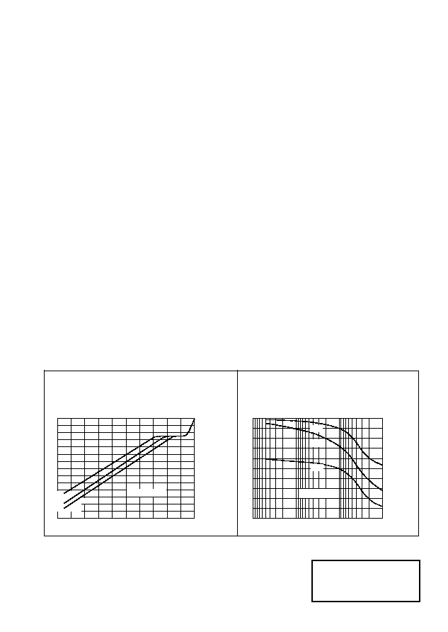
TYPICAL CHARACTERISTICS
Transfer Characteristics
I
D
- Dra
i
n Curr
ent
(Amps)
V
GS
- Gate Source
Voltage (Volts)
Saturation Characteristics
I
D
- Dra
in
Curr
ent
(Amps
)
V
DS
- Drain Source
Voltage (Volts)
Transconductance v drain current
I
D
- Drain Current (Amps
)
g
fs
-
T
ra
nsc
o
nducta
nce (mS)
Transconductance v gate-source voltage
V
GS
-Gate Source Voltage (Volts)
g
fs
-
T
ra
nsc
o
nducta
nce (mS)
Normalised R
DS(on)
and V
GS(th)
vs Temperature
Junction Temperature (�C)
N
o
rm
al
i
sed
R
D
S(
on
)
and
V
GS
(
th)
On-resistance vs Drain Current
I
D-
Drain Current
(Amps)
R
DS(o
n)-Drai
n Sour
c
e
O
n
Resi
sta
nce
(
)
I
D=
1mA
V
GS=
V
DS
0
2
4
6
8
10
0
0.2
0.4
0.6
0.8
1.0
1.2
1.4
1.6
300
�
s Pulsed Test
4V
5V
0
2
4
6
8
10
0
0.2
0.4
0.6
0.8
1.0
1.2
1.4
1.6
3V
2.5V
2V
300
�
s Pulsed Test
V
DS
=10V
-50
-25
0
25
50
75
100
125
150
0
0.4
0.8
1.2
1.6
2.4
2.0
300
�
s Pulsed Test
1.0
10
1.0
10
0.1
0.01
100
2.5V
3V
10V
V
GS
=2V
I
D
=0.5A
V
GS=
10V
0
200
400
600
800
0
0.2
0.4
0.6
0.8
1.0
1.2
1.4
0
1
2
3
4
5
0
200
400
600
800
300
�
s Pulsed Test
V
DS
=10V
300
�
s Pulsed Test
V
DS
=10Vz
V
GS
=10V
1
10
100
0.1
0
50
100
150
200
250
0
2
4
6
8
10
12
14
16
18
20
0
2
4
6
8
10
12
14
TYPICAL CHARACTERISTICS
Q-Gate Charge (nC)
Capacitance v drain-source voltage
C-C
a
p
aci
ta
n
c
e (p
F)
C
rss
C
oss
V
DS
-Drain Source Voltage (Volts)
Note:V
GS=
0V
C
iss
V
GS
-
Gat
e
Sou
r
c
e
V
o
l
t
a
g
e
(V
o
l
t
s
)
Gate charge v gate-source voltage
Note:I
D=
400mA
V
DD
= 20V
50V
100V
ZVN4424G
ZVN4424G
3 - 417
3 - 418
TYPICAL CHARACTERISTICS
Transfer Characteristics
I
D
- Dra
i
n Curr
ent
(Amps)
V
GS
- Gate Source
Voltage (Volts)
Saturation Characteristics
I
D
- Dra
in
Curr
ent
(Amps
)
V
DS
- Drain Source
Voltage (Volts)
Transconductance v drain current
I
D
- Drain Current (Amps
)
g
fs
-
T
ra
nsc
o
nducta
nce (mS)
Transconductance v gate-source voltage
V
GS
-Gate Source Voltage (Volts)
g
fs
-
T
ra
nsc
o
nducta
nce (mS)
Normalised R
DS(on)
and V
GS(th)
vs Temperature
Junction Temperature (�C)
N
o
rm
al
i
sed
R
D
S(
on
)
and
V
GS
(
th)
On-resistance vs Drain Current
I
D-
Drain Current
(Amps)
R
DS(o
n)-Drai
n Sour
c
e
O
n
Resi
sta
nce
(
)
I
D=
1mA
V
GS=
V
DS
0
2
4
6
8
10
0
0.2
0.4
0.6
0.8
1.0
1.2
1.4
1.6
300
�
s Pulsed Test
4V
5V
0
2
4
6
8
10
0
0.2
0.4
0.6
0.8
1.0
1.2
1.4
1.6
3V
2.5V
2V
300
�
s Pulsed Test
V
DS
=10V
-50
-25
0
25
50
75
100
125
150
0
0.4
0.8
1.2
1.6
2.4
2.0
300
�
s Pulsed Test
1.0
10
1.0
10
0.1
0.01
100
2.5V
3V
10V
V
GS
=2V
I
D
=0.5A
V
GS=
10V
0
200
400
600
800
0
0.2
0.4
0.6
0.8
1.0
1.2
1.4
0
1
2
3
4
5
0
200
400
600
800
300
�
s Pulsed Test
V
DS
=10V
300
�
s Pulsed Test
V
DS
=10Vz
V
GS
=10V
1
10
100
0.1
0
50
100
150
200
250
0
2
4
6
8
10
12
14
16
18
20
0
2
4
6
8
10
12
14
TYPICAL CHARACTERISTICS
Q-Gate Charge (nC)
Capacitance v drain-source voltage
C-C
a
p
aci
ta
n
c
e (p
F)
C
rss
C
oss
V
DS
-Drain Source Voltage (Volts)
Note:V
GS=
0V
C
iss
V
GS
-
Gat
e
Sou
r
c
e
V
o
l
t
a
g
e
(V
o
l
t
s
)
Gate charge v gate-source voltage
Note:I
D=
400mA
V
DD
= 20V
50V
100V
ZVN4424G