
N-CHANNEL ENHANCEMENT
MODE VERTICAL DMOS FET
ISSUE 3 - APRIL 1998
FEATURES
*
60 Volt V
DS
*
R
DS(on)
= 1
*
Repetitive avalanche rating
*
No transient protection required
*
Characterised for 5V logic drive
APPLICATIONS
*
Automotive relay drivers
*
Stepper motor driver
ABSOLUTE MAXIMUM RATINGS.
PARAMETER
SYMBOL
VALUE
UNIT
Drain-Source Voltage
V
DS
60
V
Continuous Drain Current at T
amb
=25�C
I
D
600
mA
Pulsed Drain Current
I
DM
8
A
Gate-Source Voltage
V
GS
�
20
V
Power Dissipation at T
amb
=25�C
P
tot
700
mW
Continuous Body Diode Current at T
amb
=25�C
I
SD
600
mA
Avalanche Current � Repetitive
I
AR
600
mA
Avalanche Energy � Repetitive
E
AR
15
mJ
Operating and Storage Temperature Range
T
j
:T
stg
-55 to +150
�C
ELECTRICAL CHARACTERISTICS (at T
amb
= 25�C unless otherwise stated).
PARAMETER
SYMBOL MIN.
MAX. UNIT CONDITIONS.
Drain-Source Breakdown Voltage BV
DSS
60
V
I
D
=1mA, V
GS
=0V
Gate-Source Threshold Voltage V
GS(th)
1.3
3
V
I
D
=1mA, V
DS
= V
GS
Gate-Body Leakage
I
GSS
100
nA
V
GS
=
�
20V, V
DS
=0V
Zero Gate Voltage Drain
Current
I
DSS
10
100
�
A
�
A
V
DS
=60V, V
GS
=0
V
DS
=48V, V
GS
=0V, T=125�C
(2)
On-State Drain Current(1)
I
D(on)
3
A
V
DS
=25V, V
GS
=10V
Static Drain-Source On-State
Resistance (1)
R
DS(on)
1
1.5
V
GS
=10V,I
D
=1.5A
V
GS
=5V,I
D
=.0.5A
Forward Transconductance(1)(2) g
fs
300
mS
V
DS
=25V,I
D
=1.5A
Input Capacitance (2)
C
iss
100
pF
Common Source Output
Capacitance (2)
C
oss
60
pF
V
DS
=25V, V
GS
=0V, f=1MHz
Reverse Transfer Capacitance (2) C
rss
20
pF
Turn-On Delay Time (2)(3)
t
d(on)
8
ns
V
DD
25V, I
D
=1.5A,V
GEN
=10V
Rise Time (2)(3)
t
r
12
ns
Turn-Off Delay Time (2)(3)
t
d(off)
12
ns
Fall Time (2)(3)
t
f
15
ns
(1) Measured under pulsed conditions. Width=300
�
s. Duty cycle
2% (2) Sample test.
(3) Switching times measured with 50
source impedance and <5ns rise time on a pulse generator
E-Line
TO92 Compatible
ZVN4206AV
D
G
S
ZVN4206AV
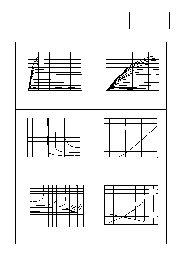
Output Characteristics
V
DS
- Drain Source
Voltage (Volts)
2
4
6
8
10
0
10
20
30
40
50
Saturation Characteristics
V
DS
- Drain Source
Voltage (Volts)
I
D
-
D
r
ain
C
urr
e
nt (Amps)
I
D
- Drain Curre
n
t (
A
mps)
0
4
2
6
10
8
10V
8V
9V
7V
5V
4V
6V
4.5V
3.5V
V
GS=
20V
12V
14V
16V
5V
4V
10V
8V
6V
9V
7V
4.5V
3.5V
V
GS=
20V
12V
14V
16V
0
4
2
6
10
8
TYPICAL CHARACTERISTICS
Transfer Characteristics
V
DS-
Dr
ai
n S
o
u
r
c
e
V
o
l
t
age (
V
o
l
t
s
)
Voltage Saturation Characteristics
V
GS-
Gate Source Voltage
(Volts)
V
GS-
Gate Source
Voltage (Volts)
0
2
4
6
8
10
6
4
0
2
I
D
-
D
r
a
i
n
C
u
r
r
e
nt (Amp
s
)
V
DS=
10V
0
10
6
2
4
8
0
2
4
6
8
10
I
D=
3A
1.5A
0.5A
On-resistance v drain current
I
D-
Drain Current
(Amps)
R
DS
(on)
-
D
rain So
u
r
ce
On
R
e
s
i
sta
n
c
e
(
)
0.1
1.0
10
4.5V
6V
V
GS
=3.5V
8V 10V
0.1
1.0
Normalised R
DS(on)
and V
GS(th)
v Temperature
T
j
-Junction Temperature (�C)
Normalised R
DS(
o
n)
a
n
d V
GS(th)
-50 -25
0
25 50 75 100
150
125
175 200
2.4
2.2
2.0
1.8
1.6
1.4
1.2
1.0
0.6
0.8
Dr
ai
n-
So
urc
e R
es
ista
nc
e
R
DS(
on
)
Gate Threshold Voltage V
GS(TH)
I
D=
1.5A
V
GS=
10V
I
D=
1mA
V
GS=
V
DS
2.6
225
20V
14V
Transfer Characteristics
V
DS-
Dr
ai
n S
o
u
r
c
e
V
o
l
t
age (
V
o
l
t
s
)
Voltage Saturation Characteristics
V
GS-
Gate Source Voltage
(Volts)
V
GS-
Gate Source
Voltage (Volts)
0
2
4
6
8
10
6
4
0
2
I
D
-
D
r
a
i
n
C
u
r
r
e
nt (Amp
s
)
V
DS=
10V
0
10
6
2
4
8
0
2
4
6
8
10
I
D=
3A
1.5A
0.5A
On-resistance v drain current
I
D-
Drain Current
(Amps)
0.1
1.0
10
4.5V
6V
V
GS
=3.5V
8V 10V
0.1
10
Normalised R
DS(on)
and V
GS(th)
v Temperature
T
j
-Junction Temperature (�C)
Normalised R
DS(
o
n)
a
n
d V
GS(th)
-50 -25
0
25 50 75 100
150
125
175 200 225
20V
14V
ZVN4206AV
V
DS
-Drain Source Voltage (Volts)
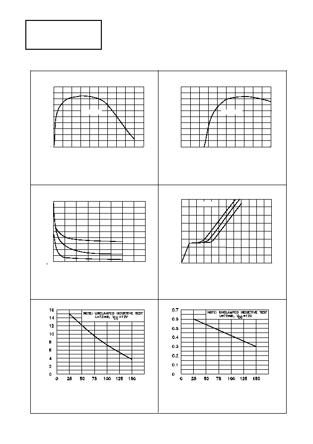
Capacitance v drain-source voltage
C-
Ca
pa
c
ita
nce
(
pF)
Q-Charge (nC)
V
G
S
-Gate S
ourc
e
V
oltage (V
olts)
Gate charge v gate-source voltage
0
10
8
6
2
0
4
12
14
16
V
DS
=
20V
I
D=
1.5A
40V 60V
0.5 1.0 1.5 2.0 2.5 3.0 3.5 4.0 4.5 5.0 5.5 6.0
C
oss
C
iss
C
rss
0
10
20
30
40
50
60
70
80
0
120
80
40
160
200
T
j
- Junction Temperature (�C)
Maximum repetative avalanche energy
v Junction Temperature
Maximum repetative avalanche current
v Junction Temperature
T
j
- Junction Temperature (�C)
E
A
R
-
R
e
pe
ta
tive A
valan
c
e
En
e
r
gy
(
mJ)
I
A
R
-
R
e
p
eta
tive A
valan
c
e
C
u
r
r
e
nt
(
A)
Transconductance v drain current
I
D
- Drain Current (Amps
)
g
f
s
-T
ransconductance (mS)
g
fs
-
T
r
an
sc
o
nd
ucta
nce
(
mS)
Transconductance v gate-source voltage
V
GS
-Gate Source Voltage (Volts)
0
1
2
3
4
5
6
7
8
9
10
V
DS=
10V
0
300
200
100
400
800
700
600
500
900
1000
0
1
2
3
4
5
6
7
8
9
10
V
DS=
10V
0
300
200
100
400
800
700
600
500
900
1000
TYPICAL CHARACTERISTICS