1
Zarlink Semiconductor Inc.
Zarlink, ZL and the Zarlink Semiconductor logo are trademarks of Zarlink Semiconductor Inc.
Copyright 2005, Zarlink Semiconductor Inc. All Rights Reserved.
A full Design Manual is available to qualified customers.
To register, please send an email to
TimingandSync@Zarlink.com.
Features
· Supports the requirements of Telcordia GR-253 and
GR-1244 for Stratum 3, 4E, 4 and SMC clocks, and
the requirements of ITU-T G.781 SETS, G.813
SEC, G.823, G.824 and G.825 clocks
· Internal APLL provides standard output clock
frequencies up to 622.08 MHz with jitter < 1 ps
RMS suitable for OC-48/STM-16 interfaces
· Programmable output synthesizers generate clock
frequencies from any multiple of 8 kHz up to
77.76 MHz in addition to 2 kHz
· Provides two DPLLs which are independently
configurable through a serial software interface
· DPLL1 provides all the features necessary for
generating SONET/SDH compliant clocks including
automatic hitless reference switching, automatic
mode selection (locked, free-run, holdover),
selectable loop bandwidth and pull-in range
· DPLL2 provides a comprehensive set of features
necessary for generating derived output clocks and
other general purpose clocks
· Provides 8 reference inputs which support clock
frequencies with any multiples of 8 kHz up to
77.76 MHz in addition to 2 kHz
· Supports master/slave configuration for
AdvancedTCA
TM
· Configurable input to output delay and output to
output phase alignment
· Optional external feedback path provides dynamic
input to output delay compensation
· Provides 3 sync inputs for output frame pulse
alignment
· Generates several styles of output frame pulses
with selectable pulse width, polarity and frequency
· Flexible input reference monitoring automatically
disqualifies references based on frequency and
phase irregularities
· Supports IEEE 1149.1 JTAG Boundary Scan
December 2005
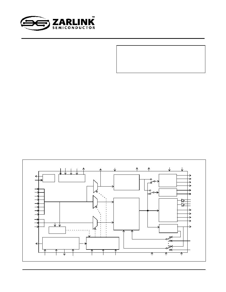
Figure 1 - Block Diagram
dpll1_mod_sel1:0
tck
tdo
tdi tms
trst_b
dpll1_holdover
dpll1_lock
DPLL2
sck
so
si
DPLL1
slave_en
dpll2_ref
rst_b
dpll1_hs_en
cs_b
diff0_en
diff1_en
Reference
Monitors
ref
sync
ref
ref0
ref1
ref2
ref3
ref4
ref5
ref6
ref7
sync0
sync1
sync2
int_b
sdh_clk0
sdh_clk1
sdh_fp0
sdh_fp1
p0_clk0
p0_clk1
p0_fp0
p0_fp1
p1_clk0
p1_clk1
fb_clk
ref7:0
sync2:0
ref_&_sync_status
Controller &
State Machine
SPI Interface
SONET/SDH
APLL
P0
Synthesizer
P1
Synthesizer
Feedback
Synthesizer
diff0
diff1
IEEE 1449.1
JTAG
Master
Clock
fb_clk
ext_fb_clk
ext_fb_fp
osco
osci
fb_fp
sdh_filter filter_ref0
filter_ref1
ZL30116
SONET/SDH
Low Jitter System Synchronizer
Data Sheet
Ordering Information
ZL30116GGG
100 Pin CABGA
Trays
ZL30116GGG2
100 Pin CABGA* Trays
*Pb Free Tin/Silver/Copper
-40
o
C to +85
o
C