DS081 (v1.2) September 4, 2001
www.xilinx.com
1
Advance Product Specification
1-800-255-7778
© 2001 Xilinx, Inc. All rights reserved. All Xilinx trademarks, registered trademarks, patents, and disclaimers are as listed at
http://www.xilinx.com/legal.htm
.
All other trademarks and registered trademarks are the property of their respective owners. All specifications are subject to change without notice.
Features
·
Lowest power 512 macrocell CPLD
·
7.5 ns pin-to-pin logic delays
·
System frequencies up to 127 MHz
·
512 macrocells with 12,800 usable gates
·
Available in small footprint packages
-
208-pin PQFP (180 user I/O)
-
256-ball FBGA (212 user I/O)
-
324-ball FBGA (260 user I/O)
·
Optimized for 3.3V systems
-
Ultra low power operation
-
5V tolerant I/O pins with 3.3V core supply
-
Advanced 0.35 micron five layer metal EEPROM
process
-
FZPTM CMOS design technology
·
Advanced system features
-
In-system programming
-
Input registers
-
Predictable timing model
-
Up to 23 clocks available per function block
-
Excellent pin retention during design changes
-
Full IEEE Standard 1149.1 boundary-scan (JTAG)
-
Four global clocks
-
Eight product term control terms per function block
·
Fast ISP programming times
·
Port Enable pin for additional I/O
·
2.7V to 3.6V supply voltage at industrial grade voltage
range
·
Programmable slew rate control per output
·
Security bit prevents unauthorized access
·
Refer to XPLA3 family data sheet (DS012) for
architecture description
Description
The XCR3512XL is a 3.3V, 512 macrocell CPLD targeted at
power sensitive designs that require leading edge program-
mable logic solutions. A total of 32 function blocks provide
12,800 usable gates. Pin-to-pin propagation delays are
7.5 ns with a maximum system frequency of 127 MHz.
TotalCMOSTM Design Technique for
Fast Zero Power
Xilinx offers a TotalCMOS CPLD, both in process technol-
ogy and design technique. Xilinx employs a cascade of
CMOS gates to implement its sum of products instead of
the traditional sense amp approach. This CMOS gate imple-
mentation allows Xilinx to offer CPLDs that are both high
performance and low power, breaking the paradigm that to
have low power, you must have low performance. Refer to
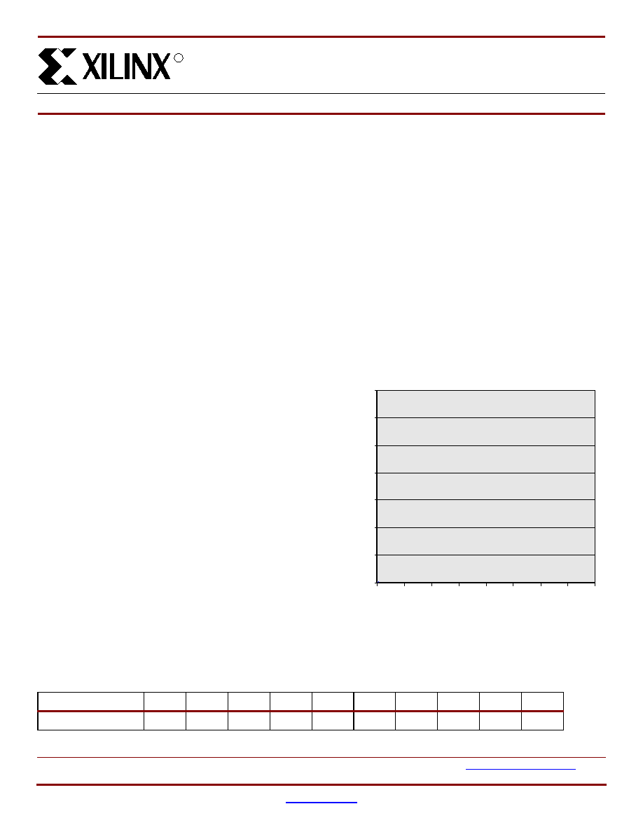
Figure 1
and
Table 1
showing the I
CC
vs. Frequency of our
XCR3512XL TotalCMOS CPLD (data taken with 32
up/down, loadable 16-bit counters at 3.3V, 25°C).
0
XCR3512XL: 512 Macrocell CPLD
DS081 (v1.2) September 4, 2001
0
14
Advance Product Specification
R
Figure 1: XCR3512XL Typical I
CC
vs. Frequency at V
CC
= 3.3V, 25
°
C
0
20
40
60
80
100
120
140
0
20
40
60
80
100
120
140
160
DS024_01_112700
Frequency (MHz)
T
yp
i
ca
l
ICC
(
m
A)
Table 1: Typical I
CC
vs. Frequency at V
CC
= 3.3V, 25
°
C
Frequency (MHz)
0
1
10
20
40
60
80
100
120
140
Typical I
CC
(mA)
TBD
TBD
TBD
TBD
TBD
TBD
TBD
TBD
TBD
TBD

XCR3512XL: 512 Macrocell CPLD
2
www.xilinx.com
DS081 (v1.2) September 4, 2001
1-800-255-7778
Advance Product Specification
R
DC Electrical Characteristics Over Recommended Operating Conditions
(1)
Symbol
Parameter
Test Conditions
Min.
Max.
Unit
V
OH
(
2
)
Output High voltage
V
CC
= 3.0V to 3.6V, I
OH
= 8 mA
2.4
-
V
V
CC
= 2.7V to 3.0V, I
OH
= 8 mA
2.0
(
3
)
-
V
I
OH
= 500
µ
A 90%
V
CC
-
V
V
OL
Output Low voltage
I
OL
= 8 mA
-
0.4
V
I
IL
Input leakage current
V
IN
= GND or V
CC
10
10
µ
A
I
IH
I/O High-Z leakage current
V
IN
= GND or V
CC
10
10
µ
A
I
CCSB
Standby current
V
CC
= 3.6V
-
100
µ
A
I
CC
Dynamic current
(
4
,
5
)
f = 1 MHz
-
TBD
mA
f = 50 MHz
-
TBD
mA
C
IN
Input pin capacitance
(
6
)
f = 1 MHz
-
8
pF
C
CLK
Clock input capacitance
(
6
)
f = 1 MHz
5
12
pF
C
I/O
I/O pin capacitance
(
6
)
f = 1 MHz
-
10
pF
Notes:
1.
See XPLA3 family data sheet (DS012) for recommended operating conditions
2.
See
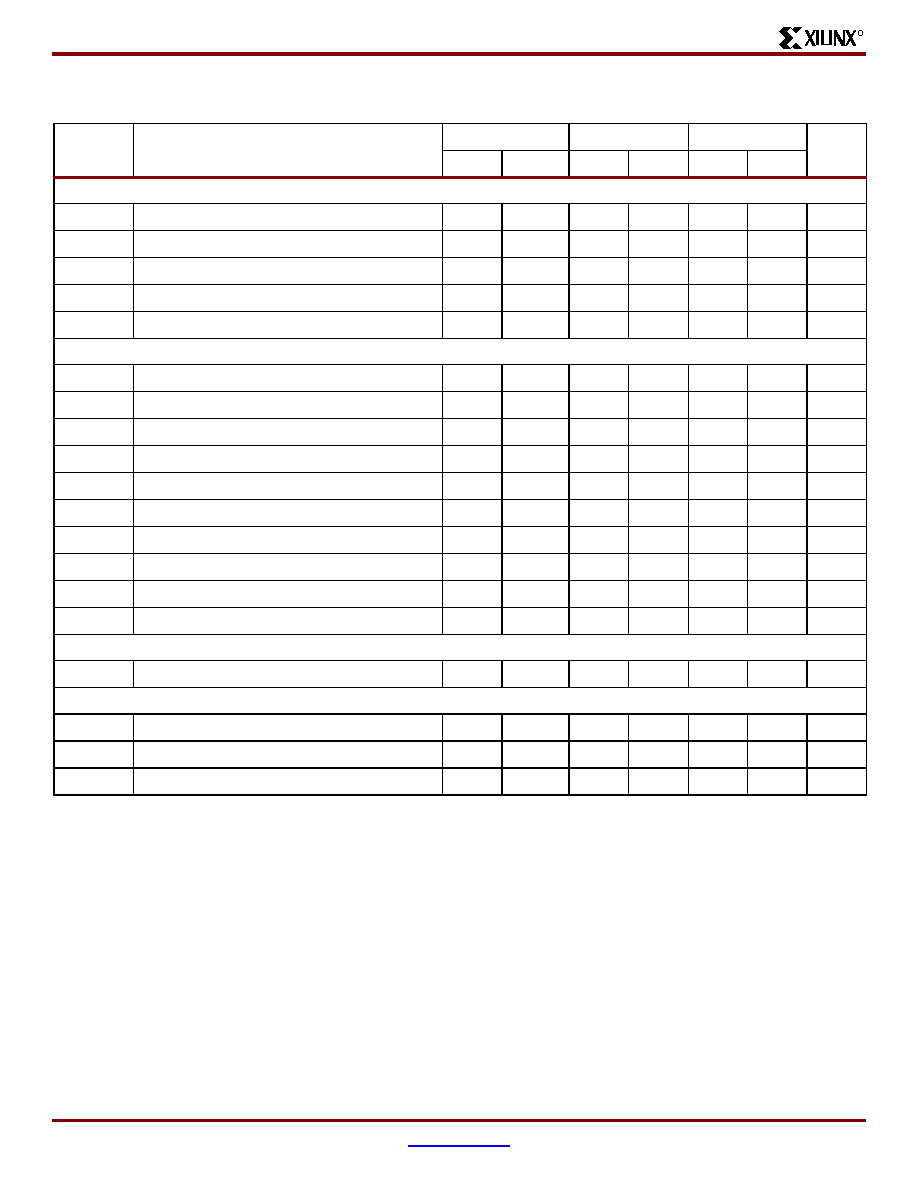
Figure 2
for output drive characteristics of the XPLA3 family.
3.
This parameter guaranteed by design and characterization, not by testing.
4.
See
Table 1
,
Figure 1
for typical values.
5.
This parameter measured with a 16-bit, loadable up/down counter loaded into every function block, with all outputs disabled and
unloaded. Inputs are tied to V
CC
or ground. This parameter guaranteed by design and characterization, not testing.
6.
Typical values, not tested.

XCR3512XL: 512 Macrocell CPLD
DS081 (v1.2) September 4, 2001
www.xilinx.com
3
Advance Product Specification
1-800-255-7778
R
AC Electrical Characteristics Over Recommended Operating Conditions
(1,2)
Figure 2: Typical I/V Curve for the XPLA3 Family
Symbol
Parameter
-7
-10
-12
Unit
Min.
Max.
Min.
Max.
Min.
Max.
T
PD1
Propagation delay time (single p-term)
-
9.0
-
10.8
ns
T
PD2
Propagation delay time (OR array)
(3)
-
10.0
-
12.0
ns
T
CO
Clock to output (global synchronous pin clock)
-
5.8
-
6.9
ns
T
SUF
(4)
Setup time fast
3.5
-
3.5
-
ns
T
SU
(4)
Setup time
6.5
-
7.9
-
ns
T
H
(4)
Hold time
0
-
0
-
ns
T
WLH
(4)
Global Clock pulse width (High or Low)
4.0
-
5.0
-
ns
Tt
PLH
(4)
P-term clock pulse width
6.0
-
7.5
-
ns
T
R
(4)
Input rise time
-
20
-
20
ns
T
L
(4)
Input fall time
-
20
-
20
ns
f
SYSTEM
(4)
Maximum system frequency
-
97
-
77
MHz
T
CONFIG
(4)
Configuration time
(5)
-
TBD
-
TBD
µ
s
T
INIT
(4)
ISP initialization time
-
TBD
-
TBD
µ
s
T
POE
(4)
P-term OE to output enabled
-
11.0
-
13.0
ns
T
POD
(4)
P-term OE to output disabled
(6)
-
11.0
-
13.0
ns
T
PCO
(4)
P-term clock to output
-
10.3
-
12.4
ns
T
PAO
(4)
P-term set/reset to output valid
-
11.0
-
13.0
ns
Notes:
1.
Specifications measured with one output switching.
2.
See XPLA3 family data sheet (DS012) for recommended operating conditions.
3.
See
Figure 4
for derating.
4.
These parameters guaranteed by design and/or characterization, not testing.
5.
Typical current draw during configuration is 12 mA at 3.6V.
6.
Output C
L
= 5 pF.
0
0
10
20
30
40
50
60
70
80
90
100
0.5
1
1.5
2
2.5
3
3.5
4
4.5
5
Volts
I
OL
(3.3V)
I
OH
(3.3V)
I
OH
(2.7V)
m
A
DS012_10_041901
XCR3512XL: 512 Macrocell CPLD
4
www.xilinx.com
DS081 (v1.2) September 4, 2001
1-800-255-7778
Advance Product Specification
R
Internal Timing Parameters
(1,2)
Symbol
Parameter
-7
-10 -12
Unit
Min.
Max.
Min.
Max.
Min.
Max.
Buffer Delays
T
IN
Input buffer delay
-
3.3
-
4.0
ns
T
FIN
Fast input buffer delay
-
3.8
-
3.8
ns
T
GCK
Global clock buffer delay
-
1.3
-
1.5
ns
T
OUT
Output buffer delay
-
3.2
-
3.8
ns
T
EN
Output buffer enable/disable delay
-
5.2
-
6.0
ns
Internal Register and Combinatorial Delays
T
LDI
Latch transparent delay
-
1.6
-
2.0
ns
T
SUI
Register setup time
1.0
-
1.2
-
ns
T
HI
Register hold time
5.5
-
6.7
-
ns
T
ECSU
Register clock enable setup time
2.5
-
3.0
-
ns
T
ECHO
Register clock enable hold time
4.5
-
5.5
-
ns
T
COI
Register clock to output delay
-
1.3
-
1.6
ns
T
AOI
Register async. S/R to output delay
-
2.0
-
2.2
ns
T
RAI
Register async. recovery
-
7.0
-
8.0
ns
T
LOGI1
Internal logic delay (single p-term)
-
2.5
-
3.0
ns
T
LOGI2
Internal logic delay (PLA OR term)
-
3.5
-
4.2
ns
Feedback Delays
T
F
ZIA delay
-
4.5
-
6.0
ns
Time Adders
T
LOGI3
Fold-back NAND delay
-
2.5
-
3.0
ns
T
UDA
Universal delay
-
2.8
-
3.5
ns
T
SLEW
Slew rate limited delay
-
5.0
-
6.0
ns
Notes:
1.
These parameters guaranteed by design and/or characterization, not testing.
2.
See XPLA3 family data sheet (DS012) for timing model.
XCR3512XL: 512 Macrocell CPLD
DS081 (v1.2) September 4, 2001
www.xilinx.com
5
Advance Product Specification
1-800-255-7778
R
Switching Characteristics
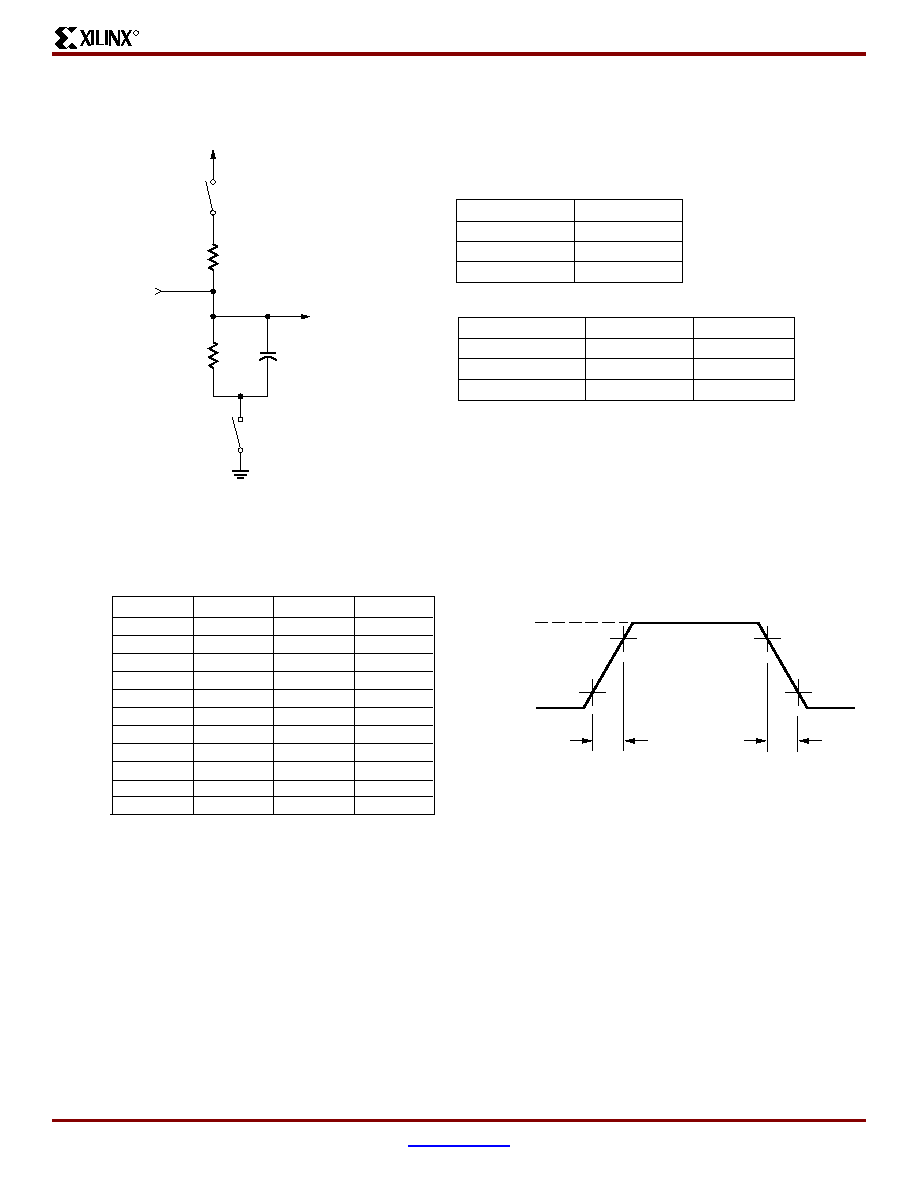
Figure 3: AC Load Circuit
VCC
V
OUT
V
IN
C1
R1
R2
S1
S2
DS013_03_050200
Component
Values
R1
390
R2
390
C1
35 pF
Measurement
S1
S2
T
POE (High)
T
POE (Low)
T
P
Open
Closed
Closed
Open
Closed
Closed
Note: For T
POD
, C1 = 5 pF
Figure 4: Derating Curve for T
PD2
6.3
6.4
6.5
6.6
6.7
6.8
6.9
7.0
7.1
7.2
7.3
7.4
7.5
1
2
4
8
16
DS024_04_11800
Number of Adjacent Outputs Switching
(ns)
Figure 5: Voltage Waveform
90%
10%
1.5 ns
1.5 ns
DS017_05_042800
+3.0V
0V
Measurements:
All circuit delays are measured at the +1.5V level of
inputs and outputs, unless otherwise specified.
T
R
T
L