
REV 1.3.13 6/19/03
1 of 12
www.xicor.com
Digitally Controlled Potentiometer (XDCP
TM
)
X93154
FEATURES
À Solid-state potentiometer
À 3-wire serial interface
À 32 wiper tap points
--Wiper position stored in nonvolatile memory
and recalled on power-up
À 31 resistive elements
--Temperature compensated
--End to end resistance range ▒ 30%
--Terminal voltage, 0 to V
CC
À Low power CMOS
--V
CC
= 3V▒10%
--Active current, 250ÁA max.
--Standby current, 1ÁA max.
À High reliability
--Endurance 20,000 data changes per bit
--Register data retention, 10 years
À R
TOTAL
value = 50K
À Packages
--8-lead MSOP, FCP
DESCRIPTION
The Xicor X93154 is a digitally controlled potentiome-
ter (XDCP). The device consists of a resistor array,
wiper switches, a control section, and nonvolatile
memory. The wiper position is controlled by a 3-wire
interface.
The potentiometer is implemented by a resistor array
composed of 31 resistive elements and a wiper switch-
ing network. The position of the wiper element is con-
trolled by the CS, U/D, and INC inputs. The position of
the wiper can be stored in nonvolatile memory and
then be recalled upon a subsequent power-up opera-
tion.
The device is connected as a two-terminal variable
resistor and can be used in a wide variety of applica-
tions including:
¡ bias and gain control
¡ LCD Contrast Adjustment
A
PPLICATION
N
OTE
A V A I L A B L E
AN20 À AN42¡53 À AN71 À AN73 À AN88 À AN91¡92 À AN99 À AN115 À AN120 À AN124 À AN133 À AN134 À AN135
XDCP
TM
is a trademark of Xicor, Inc.
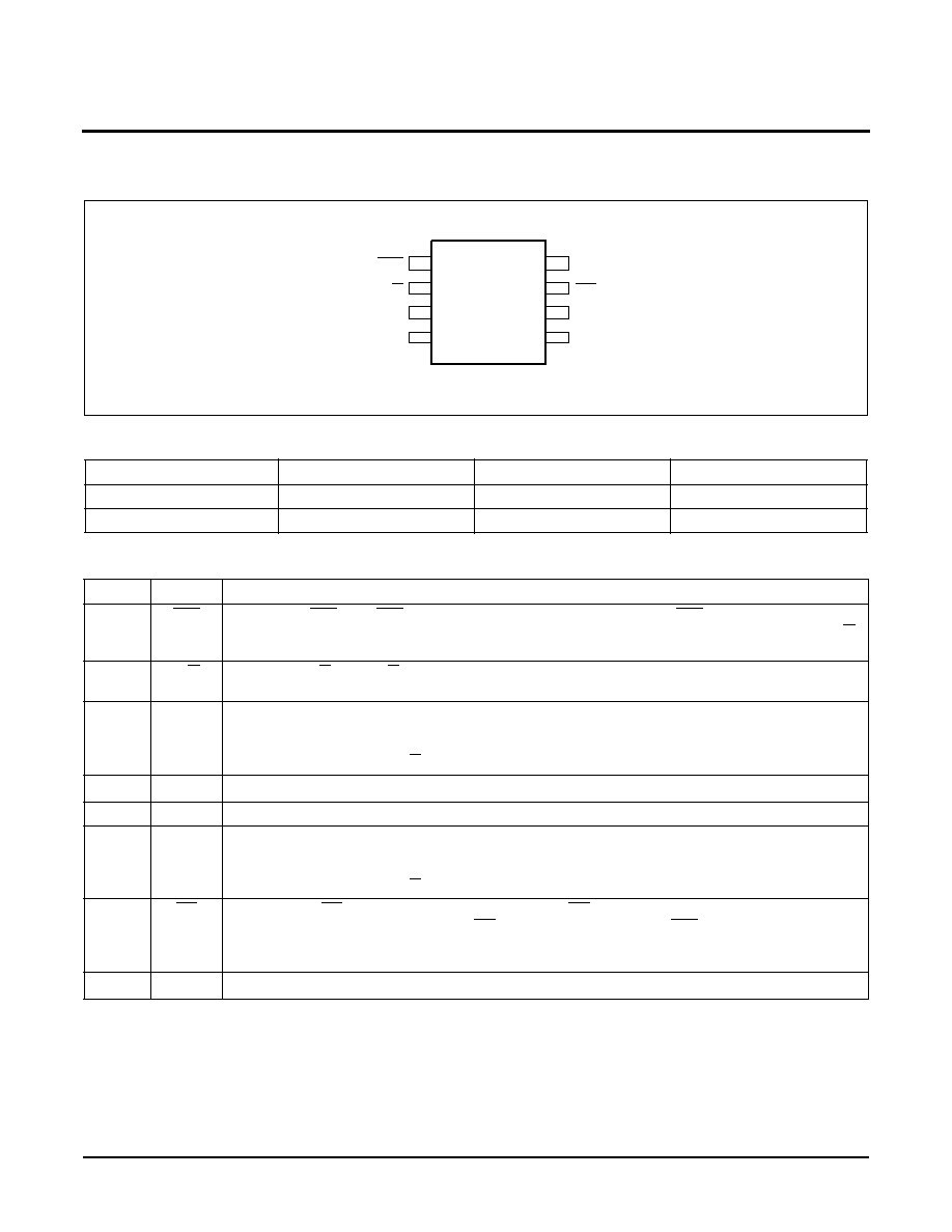
Low Noise, Low Power, 32 Taps
BLOCK DIAGRAM
5-Bit
Up/Down
Counter
5-Bit
Nonvolatile
Memory
Store and
Recall
Control
Circuitry
One
of
Decoder
Resistor
Array
R
H
U/D
INC
CS
Transfer
Gates
Thirty
V
CC
V
SS
R
L
Control
and
Memory
Up/Down
(U/D)
Increment
(INC)
Device Select
(CS)
V
CC
(Supply Voltage)
V
SS
(Ground)
R
H
General
Detailed
0
1
2
28
29
30
31
Two
R
L
30K
2 of 12
REV 1.3.13 6/19/03
www.xicor.com
X93154
PIN CONFIGURATION
X93154 ORDERING CODES
PIN DESCRIPTIONS
Ordering Number
RTOTAL
Package
Temperature Range
X93154UX8I-3
50Kohm
8-bump Flipchip package
-40░C to +85░C
X93154UM8I-3
50Kohm
8-lead MSOP package
-40░C to +85░C
MSOP
Symbol
Brief Description
1
INC
Increment (INC)
. The INC input is negative-edge triggered. Toggling INC will move the wiper and
either increment or decrement the counter in the direction indicated by the logic level on the U/D
input.
2
U/D
Up/Down (U/D)
. The U/D input controls the direction of the wiper movement and whether the
counter is incremented or decremented.
3
R
H
R
H
. The R
H
and R
L
pins of the X93154 are equivalent to the fixed terminals of a
mechanical potentiometer. The minimum voltage is V
SS
and the maximum is V
CC
. The terminol-
ogy of R
H
and R
L
references the relative position of the terminal in relation to wiper movement
direction selected by the U/D input.
4
V
SS
Ground
.
5
NC
No Connection
. (or can be connected to any voltage between V
SS
and V
CC
.)
6
R
L
R
L
. The R
H
and R
L
pins of the X93154 are equivalent to the fixed terminals of a
mechanical potentiometer. The minimum voltage is V
SS
and the maximum is V
CC
. The terminol-
ogy of R
H
and R
L
references the relative position of the terminal in relation to wiper movement
direction selected by the U/D input.
7
CS
Chip Select (CS)
. The device is selected when the CS input is LOW. The current counter value
is stored in nonvolatile memory when CS is returned HIGH while the INC input is also HIGH. After
the store operation is complete, the X93154 will be placed in the low power standby mode until
the device is selected once again.
8
V
CC
Supply Voltage
.
V
CC
CS
INC
U/D
R
H
V
SS
1
2
3
4
8
7
6
5
X93154
MSOP
R
L
NC
*
*
NC can be left unconnected, or connected to any voltage between V
SS
and V
CC
.

3 of 12
REV 1.3.13 6/19/03
www.xicor.com
X93154
ABSOLUTE MAXIMUM RATINGS
Temperature under bias ....................¡65
░
C to +135
░
C
Storage temperature ........................ ¡65░C to +150░C
Voltage on CS, INC, U/D, R
H
, R
L
and V
CC
with respect to V
SS
..............................¡1V to +6.5V
Lead temperature (soldering 10 seconds)......... 300░C
Maximum resistor current..................................... 2mA
COMMENT
Stresses above those listed under "Absolute Maximum
Ratings" may cause permanent damage to the device.
This is a stress rating only; the functional operation of
the device (at these or any other conditions above
those listed in the operational sections of this specifi-
cation) is not implied. Exposure to absolute maximum
rating conditions for extended periods may affect
device reliability.
RECOMMENDED OPERATING CONDITIONS
POTENTIOMETER CHARACTERISTICS
(Over recommended operating conditions unless otherwise stated.)
Notes:
(1) Absolute linearity is utilized to determine actual wiper voltage versus expected voltage = (V
H(n)
(actual)¡V
H(n)
(expected)) = ▒1 Ml
Maximum. n = 1 .. 29 only
(2) Relative linearity is a measure of the error in step size between taps = V
H(n+1)
--[V
H(n)
+ Ml] = ▒0.5 Ml, n = 1 .. 29 only.
(3) 1 Ml = Minimum Increment = R
TOT
/31.
(4) Typical values are for T
A
= 25░C and nominal supply voltage.
(5) This parameter is periodically sampled and not 100% tested
(6) Typical values are for T
A
= 25░C and nominal supply voltage.
(7) This parameter is not 100% tested.
(8) When performing multiple write operations, V
CC
must not decrease by more than 150mV from its initial value.
Temperature
Min.
Max.
Industrial
¡40░C
+85░C
Supply Voltage (V
CC
)
Limits
X9315
4
3V ▒10%
(8)
Symbol
Parameter
Limits
Test Conditions/Notes
Min.
Typ.
Max.
Unit
R
TOT
End to end resistance
35
50
65
K
V
R
R
H
, R
L
terminal voltages
0
V
CC
V
Power rating
1
mW
(7)
R
TOTAL
=
50 K
Noise
-120
dBV
(7)
Ref: 1kHz
R
W
Wiper Resistance
1000
(5) (6)
I
W
Wiper Current
0.6
mA
(5) (6)
Resolution
3
%
Absolute linearity
(1)
▒1
MI
(3)
V
H(n)(actual)
¡V
H(n)(expected)
Relative linearity
(2)
▒0.5
MI
(3)
V
H(n+1)
¡[V
H(n)+MI
]
R
TOTAL
temperature coefficient
▒100
ppm/░C
(7)
C
H
/C
L
/C
W
Potentiometer capacitances
10/10/25
pF
(7)
See circuit #3

X93154
4 of 12
REV 1.3.13 6/19/03
www.xicor.com
D.C. OPERATING CHARACTERISTICS (Over recommended operating conditions unless otherwise specified.)
ENDURANCE AND DATA RETENTION
Test Circuit #1
Circuit #2 SPICE Macro Model
A.C. CONDITIONS OF TEST
Symbol
Parameter
Limits
Unit
Test Conditions
Min.
Typ.
(4)
Max.
I
CC1
V
CC
active current (Increment)
50
250
ÁA
CS = V
IL
, U/D = V
IL
or V
IH
and
INC = 0.4V @ max. t
CYC
I
CC2
V
CC
active current (Store)
(EEPROM Store)
600
ÁA
CS = V
IH
, U/D = V
IL
or V
IH
and
INC = V
IH
@ max. t
WR
I
SB
Standby supply current
1
ÁA
CS = V
CC
¡ 0.3V, U/D and
INC = V
SS
or V
CC
¡ 0.3V
I
LI
CS
▒1
ÁA
V
IN
= V
CC
I
LI
CS
60
100
150
ÁA
V
CC
= 3V, CS = 0
I
LI
INC, U/D input leakage current
▒1
ÁA
V
IN
= V
SS
to V
CC
V
IH
CS, INC, U/D input HIGH voltage
V
CC
x 0.7
V
CC
+ 0.5
V
V
IL
CS, INC, U/D input LOW voltage
¡0.5
V
CC
x 0.1
V
C
IN
(5)(7)
CS, INC, U/D input capacitance
10
pF
V
CC
= 3V, V
IN
= V
SS
,
T
A
= 25░C, f = 1MHz
Parameter
Min.
Unit
Minimum endurance
20,000
Data changes per bit
Data retention
10
Years
V
L
Test Point
V
H
/R
H
C
H
C
L
10pF
10pF
R
H
R
TOTAL
C
W
25pF
R
L
Input pulse levels
0V to 3V
Input rise and fall times
10ns
Input reference levels
1.5V
5 of 12
REV 1.3.13 6/19/03
www.xicor.com
X93154
A.C. OPERATING CHARACTERISTICS (Over recommended operating conditions unless otherwise specified)
POWER UP AND DOWN REQUIREMENTS
There are no restrictions on the power-up or power-down conditions of V
CC
and the voltages applied to the potenti-
ometer pins provided that V
CC
is always more positive than or equal to V
H
and V
L
, i.e., V
CC
V
H,
V
L
. The V
CC
ramp
rate spec is always in effect.
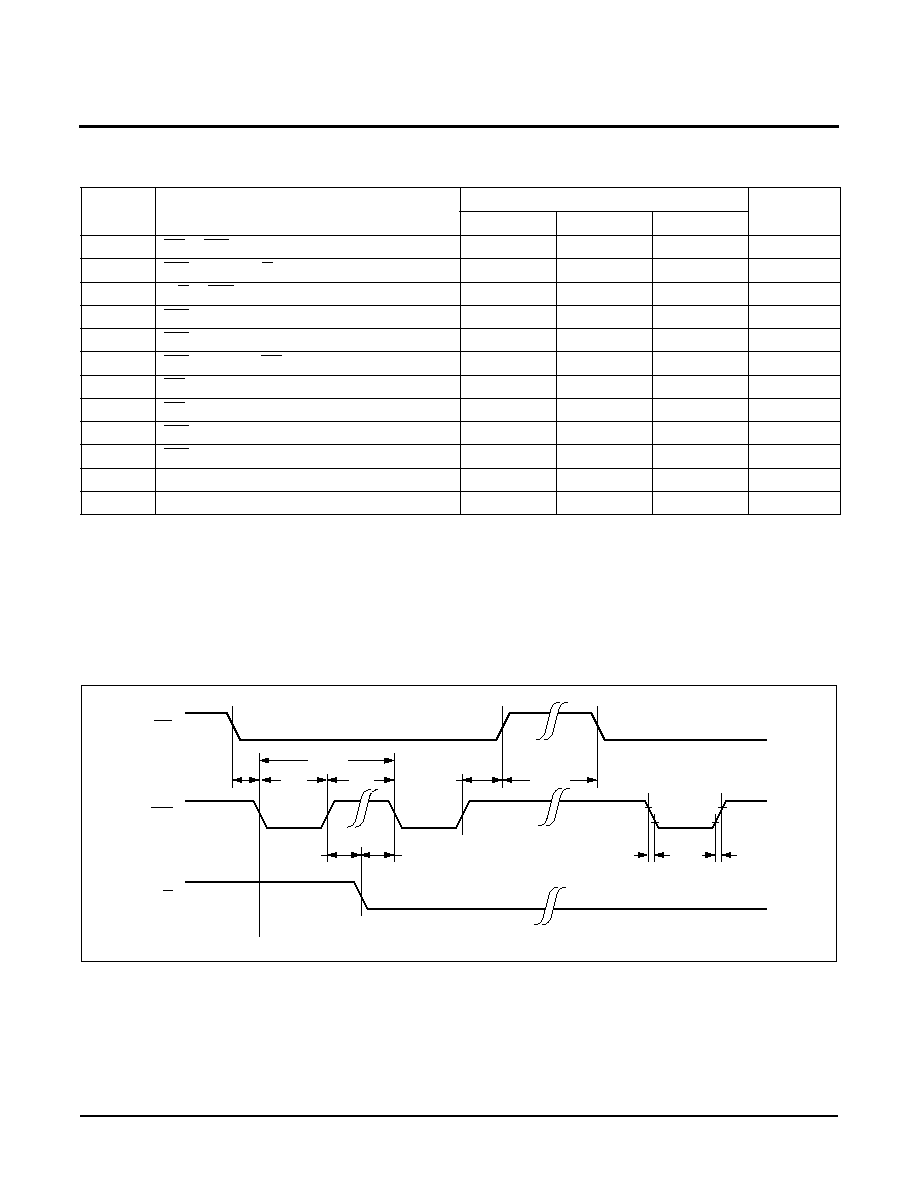
A.C. TIMING
Symbol
Parameter
Limits
Unit
Min.
Typ.
(6)
Max.
t
Cl
CS to INC setup
100
ns
t
lD
INC HIGH to U/D change
100
ns
t
DI
U/D to INC setup
100
ns
t
lL
INC LOW period
1
Ás
t
lH
INC HIGH period
1
Ás
t
lC
INC Inactive to CS inactive
1
Ás
t
CPH
CS Deselect time (NO STORE)
250
ns
t
CPH
CS Deselect time (STORE)
10
ms
t
CYC
INC cycle time
2
Ás
t
R,
t
F
(7)
INC input rise and fall time
500
Ás
t
R
V
CC
(7)
V
CC
power-up rate
1.0
10,000
V/ms
t
WR
Store cycle
5
10
ms
CS
INC
U/D
t
CI
t
IL
t
IH
t
CYC
t
ID
t
DI
t
IC
t
CPH
t
F
t
R
10%
90%
90%
(Store)
X93154
6 of 12
REV 1.3.13 6/19/03
www.xicor.com
PIN DESCRIPTIONS
R
H
and R
L
The R
H
and R
L
pins of the X93154 are equivalent to
the fixed terminals of a mechanical potentiometer. The
minimum voltage is V
SS
and the maximum is V
CC
. The
terminology of R
H
and R
L
references the relative posi-
tion of the terminal in relation to wiper movement direc-
tion selected by the U/D input.
Up/Down (U/D)
The U/D input controls the direction of the wiper move-
ment and whether the counter is incremented or decre-
mented.
Increment (INC)
The INC input is negative-edge triggered. Toggling INC
will move the wiper and either increment or decrement
the counter in the direction indicated by the logic level
on the U/D input.
Chip Select (CS)
The device is selected when the CS input is LOW. The
current counter value is stored in nonvolatile memory
when CS is returned HIGH while the INC input is also
HIGH. After the store operation is complete the
X93154 will be placed in the low power standby mode
until the device is selected once again.
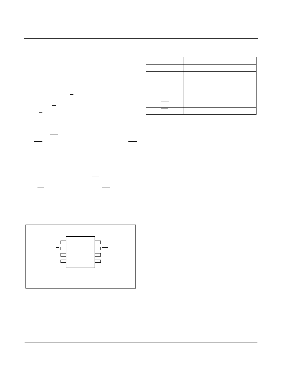
PIN CONFIGURATION
PIN NAMES
PRINCIPLES OF OPERATION
There are three sections of the X93154: the input con-
trol, counter and decode section; the nonvolatile mem-
ory; and the resistor array. The input control section
operates just like an up/down counter. The output of
this counter is decoded to turn on a single electronic
switch connecting a point on the resistor array to the
wiper output. Under the proper conditions the contents
of the counter can be stored in nonvolatile memory and
retained for future use. The resistor array is comprised
of 31 individual resistors connected in series. At either
end of the array and between each resistor is an elec-
tronic switch that transfers the connection at that point
to the wiper.
The wiper, when at either fixed terminal, acts like its
mechanical equivalent and does not move beyond the
last position. That is, the counter does not wrap around
when clocked to either extreme.
If the wiper is moved several positions, multiple taps
are connected to the wiper for t
IW
(INC to V
W
change).
The 2-terminal resistance value for the device can tem-
porarily change by a significant amount if the wiper is
moved several positions.
When the device is powered-down, the last wiper posi-
tion stored will be maintained in the nonvolatile mem-
ory. When power is restored, the contents of the
memory are recalled and the wiper is set to the value
last stored.
V
CC
CS
INC
U/D
R
H
/V
H
V
SS
1
2
3
4
8
7
6
5
X93154
MSOP
R
L
/V
L
NC
*
*
NC = No Connect. Can be connected to any
voltage between V
SS
and V
CC
, or left unconnected.
Symbol
Description
R
H
High terminal
R
L
Low terminal
V
SS
Ground
V
CC
Supply voltage
U/D
Up/Down control input
INC
Increment control input
CS
Chip Select control input

7 of 12
REV 1.3.13 6/19/03
www.xicor.com
X93154
INSTRUCTIONS AND PROGRAMMING
The INC, U/D and CS inputs control the movement of
the wiper along the resistor array. With CS set LOW the
device is selected and enabled to respond to the U/D
and INC inputs. HIGH to LOW transitions on INC will
increment or decrement (depending on the state of the
U/D input) a five bit counter. The output of this counter
is decoded to select one of thirty two wiper positions
along the resistive array.
The value of the counter is stored in nonvolatile mem-
ory whenever CS transitions HIGH while the INC input
is also HIGH. In order to avoid an accidental store dur-
ing power-up, CS must go HIGH with V
CC
during initial
power-up. When performing multiple write operations,
V
CC
must not decrease by more than 150mV from its
initial value. When left open, the CS pin is internally
pulled up to V
CC
by an internal 30K resistor.
The system may select the X93154, move the wiper
and deselect the device without having to store the lat-
est wiper position in nonvolatile memory. After the
wiper movement is performed as described above and
once the new position is reached, the system must
keep INC LOW while taking CS HIGH. The new wiper
position will be maintained until changed by the system
or until a power-up/down cycle recalled the previously
stored data. In order to recall the stored position of the
wiper on power-up, the CS pin must be held HIGH.
This procedure allows the system to always power-up
to a preset value stored in nonvolatile memory; then
during system operation minor adjustments could be
made. The adjustments might be based on user prefer-
ence, system parameter changes due to temperature
drift, or other system trim requirements.
The state of U/D may be changed while CS remains
LOW. This allows the host system to enable the device
and then move the wiper up and down until the proper
trim is attained.
MODE SELECTION
SYMBOL TABLE
CS
INC
U/D
Mode
L
H
Wiper Up
L
L
Wiper Down
H
X
Store Wiper Position
H
X
X
Standby Current
L
X
No Store, Return to Standby
L
H
Wiper Up (not recommended)
L
L
Wiper Down (not recommended)
WAVEFORM
INPUTS
OUTPUTS
Must be
steady
Will be
steady
May change
from Low to
High
Will change
from Low to
High
May change
from High to
Low
Will change
from High to
Low
Don't Care:
Changes
Allowed
Changing:
State Not
Known
N/A
Center Line
is High
Impedance

8 of 12
REV 1.3.13 6/19/03
www.xicor.com
X93154
APPLICATIONS INFORMATION
Electronic digitally controlled (XDCP) potentiometers provide three powerful application advantages; (1) the
variability and reliability of a solid-state potentiometer (2) the flexibility of computer-based digital controls, and
(3) the retentivity of nonvolatile memory used for the storage of multiple potentiometer settings or data.
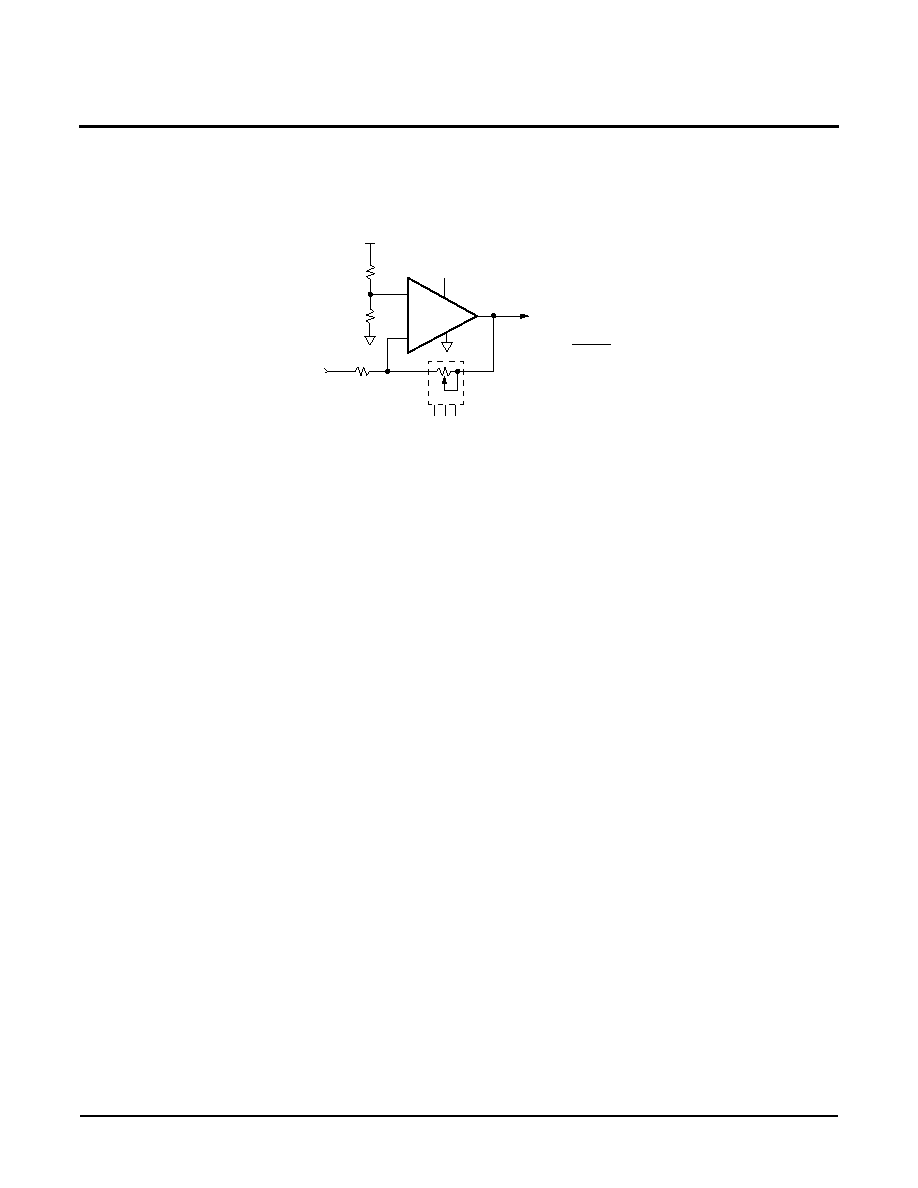
Low Voltage High Impedance Instrumentation Amplifier
Micro-Power LCD Contrast Control
V
R
Two terminal variable resistor.
I
+
¡
U1A
10k
50k
¡
+
U1C
Gain =
50k
10k
1 +
50k
R
TOTAL
)
(
U1 = LT1467
V
OUT
50k
¡
+
U1B
10k
50k
50k
X93154 (R
TOTAL
)
10k
+
10k
¡
V
IN
3.3V
+
¡
U1A
100k
300k
¡
+
U1B
1 +
100k
50k + R
TOTAL
)
(
U1 = LMC6042
V
OUT
= -3.88
¡12V
100k
X93154 (R
TOTAL
)
240k
3.3V
100k
3.3V
50k
V
OUT
= -2.75V to -11.6V
9 of 12
REV 1.3.13 6/19/03
www.xicor.com
X93154
APPLICATIONS INFORMATION (Continued)
Single Supply Variable Gain Amplifier
Gain =
R
TOTAL
10k
+
¡
U1
20k
3.3V
20k
3.3V
V
OUT
U1 = LMC6042
10k
V
IN
X93154
(R
TOTAL
)
10 of 12
REV 1.3.13 6/19/03
www.xicor.com
X93154
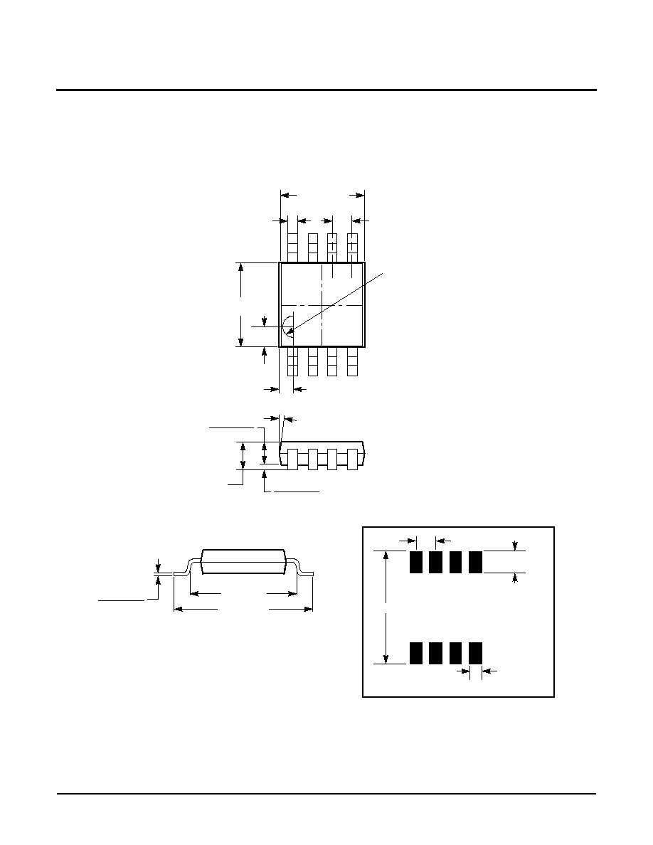
PACKAGING INFORMATION
0.118 ▒ 0.002
(3.00 ▒ 0.05)
0.040 ▒ 0.002
(1.02 ▒ 0.05)
0.150 (3.81)
Ref.
0.193 (4.90)
0.030 (0.76)
0.036 (0.91)
0.032 (0.81)
0.007 (0.18)
0.005 (0.13)
0.008 (0.20)
0.004 (0.10)
0.0216 (0.55)
7░ Typ.
R 0.014 (0.36)
0.118 ▒ 0.002
(3.00 ▒ 0.05)
0.012 + 0.006 / -0.002
(0.30 + 0.15 / -0.05)
0.0256 (0.65) Typ.
8-Lead Miniature Small Outline Gull Wing Package Type M
NOTE:
1. ALL DIMENSIONS IN INCHES AND (MILLIMETERS)
0.220"
0.0256" Typical
0.025"
Typical
0.020"
Typical
8 Places
FOOTPRINT
Ref.

11 of 12
REV 1.3.13 6/19/03
www.xicor.com
X93154
8 BUMP FCP PACKAGE
Symbol
Min
Nominal
Max
Millimeters
Package Width
A
0.960
0.990
1.020
Package Length
B
0.940
0.970
1.000
Package Height
C
0.700
0.730
0.760
Body Thickness
D
0.620
0.630
0.640
Ball Height
E
0.085
0.100
0.115
Ball Diameter
F
0.100
0.115
0.130
Bump Name
X coordinate, Ám
Y coordinate, Ám
1
INCb
-153.70
377.00
2
Vcc
257.50
375.60
3
UDb
-382.00
123.20
4
CSb
382.00
114.50
5
RL
382.00
-136.30
6
RH
-382.00
-275.10
7
Vss
-115.30
-377.00
8
NC
190.10
-377.00
a
b
c
d
f
e
e
Bottom View (Bumped Side)
Side View
Side View
1 2
3
4
6
5
7
8
AGH
YWW

Characteristics subject to change without notice.
12 of 12
LIMITED WARRANTY
Devices sold by Xicor, Inc. are covered by the warranty and patent indemnification provisions appearing in its Terms of Sale only. Xicor, Inc. makes no warranty,
express, statutory, implied, or by description regarding the information set forth herein or regarding the freedom of the described devices from patent infringement.
Xicor, Inc. makes no warranty of merchantability or fitness for any purpose. Xicor, Inc. reserves the right to discontinue production and change specifications and prices
at any time and without notice.
Xicor, Inc. assumes no responsibility for the use of any circuitry other than circuitry embodied in a Xicor, Inc. product. No other circuits, patents, or licenses are implied.
TRADEMARK DISCLAIMER:
Xicor and the Xicor logo are registered trademarks of Xicor, Inc. AutoStore, Direct Write, Block Lock, SerialFlash, MPS, BiasLock and XDCP are also trademarks of
Xicor, Inc. All others belong to their respective owners.
U.S. PATENTS
Xicor products are covered by one or more of the following U.S. Patents: 4,326,134; 4,393,481; 4,404,475; 4,450,402; 4,486,769; 4,488,060; 4,520,461; 4,533,846;
4,599,706; 4,617,652; 4,668,932; 4,752,912; 4,829,482; 4,874,967; 4,883,976; 4,980,859; 5,012,132; 5,003,197; 5,023,694; 5,084,667; 5,153,880; 5,153,691;
5,161,137; 5,219,774; 5,270,927; 5,324,676; 5,434,396; 5,544,103; 5,587,573; 5,835,409; 5,977,585. Foreign patents and additional patents pending.
LIFE RELATED POLICY
In situations where semiconductor component failure may endanger life, system designers using this product should design the system with appropriate error detection
and correction, redundancy and back-up features to prevent such an occurrence.
Xicor's products are not authorized for use in critical components in life support devices or systems.
1. Life support devices or systems are devices or systems which, (a) are intended for surgical implant into the body, or (b) support or sustain life, and whose failure to
perform, when properly used in accordance with instructions for use provided in the labeling, can be reasonably expected to result in a significant injury to the user.
2. A critical component is any component of a life support device or system whose failure to perform can be reasonably expected to cause the failure of the life
support device or system, or to affect its safety or effectiveness.
®Xicor, Inc. 2003 Patents Pending
REV 1.3.13 6/19/03
www.xicor.com
X93154