WMS7204
- 2 -
1. GENERAL DESCRIPTION
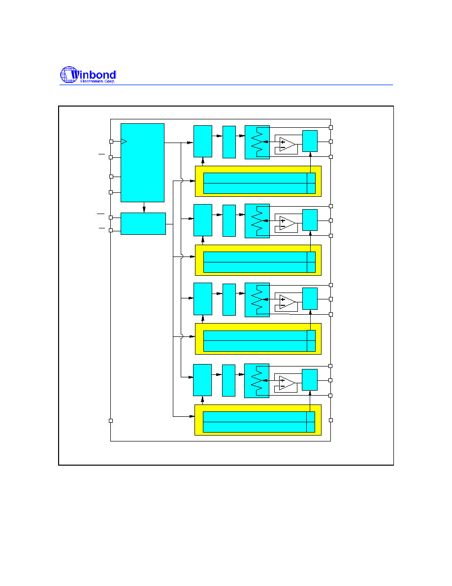
The WMS7204 is a 256-tap, quad-channel non-volatile digital potentiometer available in 10K
, 50K
and 100K
end-to-end resistances. These devices can be used as a three-terminal potentiometer or
as a two terminal variable resistor in a wide variety of applications.
The output of each potentiometer is determined by the wiper position, which varies linearly between
VA and VB terminal according to the content stored in the volatile Tap Register (TR). The settings of
the TR can be provided either directly by the user through the industry standard SPI interface, or by
the non-volatile memory (NVMEM0~3) where the previous settings are stored. When changes are
made to the TR to establish a new wiper position, the value of the setting can be saved into any non-
volatile memory location (NVMEM0~3) by executing a NVMEM save operation. Each channel has its
own four non-volatile memory locations (NVMEM0~3) that can be directly written to, and read by,
users through the SPI interface. Upon powerup the content of the NVMEM0 is automatically loaded to
the Tap Register.
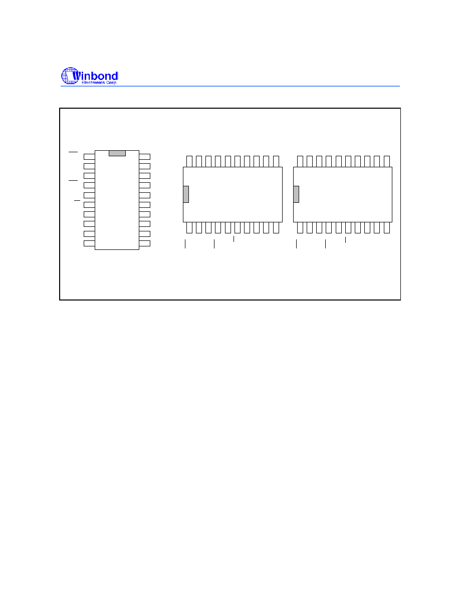
The WMS7204 contains four independent channels in 20-pin PDIP, SOIC and TSSOP packages and
can operate over a wide operating voltage range from 2.7V to 5.5V. A selectable output buffer is built-
in for each channel for those applications where an output buffer is required.
2. FEATURES
�
256 taps for each potentiometer
�
Four independent, linear-taper channels in one package
�
End-to-end resistance available in 10K
, 50K and 100K
�
Selectable output buffer for each channel
�
SPI Serial Interface for data transfer and potentiometer control
�
Daisy-chain operation for multiple devices
�
Nonvolatile storage of four wiper positions per channel with power-on recall from NVMEM0
�
Low standby current (1
�A Max. with output buffer inactive)
�
Endurance 100K typical stores per bit
�
Register Data Retention 100 years
�
Industrial temperature range: -40 ~ 85
�C
�
Wide operating voltage range: 2.7V ~ 5.5V
�
Package option:
20-pin TSSOP, 20-pin SOIC, 20-pin PDIP

WMS7204
- 4 -
4. TABLE OF CONTENTS
1. GENERAL DESCRIPTION.................................................................................................................. 2
2. FEATURES ......................................................................................................................................... 2
3. BLOCK DIAGRAM .............................................................................................................................. 3
4. TABLE OF CONTENTS ...................................................................................................................... 4
5. PIN CONFIGURATION ....................................................................................................................... 5
6. PIN DESCRIPTION............................................................................................................................. 6
7. FUNCTIONAL DESCRIPTION............................................................................................................ 8
7.1. Potentiometer and Rheostat Modes ............................................................................................. 8
7.1.1. Rheostat Configuration .......................................................................................................... 8
7.1.2. Potentiometer Configuration .................................................................................................. 8
7.2. Programming Modes .................................................................................................................... 8
7.3. Non-Volatile Memory (NVMEM) ................................................................................................... 9
7.3.1 Write Protect of NVMEM ......................................................................................................... 9
7.4 Flow Control................................................................................................................................... 9
7.5. Daisy Chain ................................................................................................................................ 10
7.6. Serial Data Interface ................................................................................................................... 11
7.7. Instruction Set............................................................................................................................. 12
7.8. Basic Operation .......................................................................................................................... 13
7.8.1 Sending a Command ............................................................................................................ 14
7.8.2 Wake Up/Sleep/Power Commands ...................................................................................... 14
7.8.3 Write to Tap Register (TR).................................................................................................... 14
7.8.4 Programming Non-Volatile Memory (NVMEM)..................................................................... 16
7.8.5 Reading Tap Registers and NVMEM Locations ................................................................... 17
8. TIMING DIAGRAMS.......................................................................................................................... 18
9. ABSOLUTE MAXIMUM RATINGS.................................................................................................... 20
10. ELECTRICAL CHARACTERISTICS ............................................................................................... 21
10.1 Test Circuits............................................................................................................................... 23
11. TYPICAL APPLICATION CIRCUIT................................................................................................. 24
11.1. Layout Considerations.............................................................................................................. 27
12. PACKAGE DRAWINGS AND DIMENSIONS.................................................................................. 28
13. ORDERING INFORMATION........................................................................................................... 31
14. VERSION HISTORY ....................................................................................................................... 32