Document Outline
- Main Menu
- Memory Products
- Search
- Web

W946432AD
512K
×
×
4 BANKS
×
×
32 BITS DDR SDRAM
PRELIMINARY DATA:9/8/00
1
GENERAL DESCRIPTION
The W946432AD is a high-speed CMOS Double Data Rate synchronous dynamic random access
memory organized as 512K words x 4 banks x 32 bits.
A bidirectional data strobe (DQS) is transmitted externally, along with data, for use in data capture at
the receiver. DQS is a strobe transmitted by the DDR SDRAM during READs and by the memory
controller during WRITEs. DQS is edge-aligned with data for READs and center-aligned with data for
WRITEs.
The W946432AD operates from a differential clock (CLK and CLK the crossing of CLK going HIGH
and CLK going LOW will be referred to as the postive edge of CLK). Commands (address and control
signals) are registered at every positive edge of CLK. Input data is registered on both edges of DQS,
and output data is referenced to both edges of DQS, as well as to both edges of CLK.
Read and write accesses to the DDR SDRAM are burst oriented; accesses start at a selected location
and continue for a programmed number of locations in a programmed sequence. Accesses begin with
the registration of an ACTIVE command, which is then followed by a READ or WRITE command. The
address bits registered coincident with the ACTIVE command are used to select the bank and row to
be accessed. The address bits registered coincident with the READ or WRITE command are used to
select the bank and the starting column location for the burst access.
The DDR SDRAM provides for programmable READ or WRITE burst lengths of 2, 4 or 8 locations. An
AUTO PRECHARGE function may be enabled to provide a self-timed row precharge that is initiated at
the end of the burst access.
As with standard SDRAMs, the pipelined, multibank architecture of DDR SDRAMs allows for
concurrent operation, thereby providing high effective bandwidth by hiding row precharge and
activation time.
FEATURES
·
Double-data-rate architecture; two data transfers
per clock cycle
·
Bidirectional, data strobe (DQS) is transmitted/
received with data, to be used in capturing data
at the receiver
·
DQS is edge-aligned with data for READs;
center-aligned with data for WRITEs
·
Differential clock inputs (CLK and CLK )
·
DLL aligns DQ and DQS transitions with CLK
transitions
·
Programmable DLL on or DLL off mode
·
Commands entered on each positive CLK edge;
data and data mask referenced to both edges of
DQS
·
Four internal banks for concurrent operation
·
Data mask (DM) for write data
·
Burst lengths: 2, 4, or 8
·
CAS Latency: 3
·
AUTO PRECHARGE option for each burst
access
·
Auto Refresh and Self Refresh Modes
·
15.6us Maximum Average Periodic Refresh
Interval
·
2.5V (SSTL_2 compatible) I/O
·
V
DD
Q = 2.5V ± 0.2V
·
V
DD
= 2.5V ± 0.2V

W946432AD
512K
×
×
4 BANKS
×
×
32 BITS DDR SDRAM
PRELIMINARY DATA:9/8/00
2
PIN CONFIGURATION
10
15
20
1
2
3
4
5
6
7
8
9
11
12
13
14
16
17
18
19
21
22
23
24
25
26
27
28
29
30
71
66
61
80
79
78
77
76
75
74
73
72
70
69
68
67
65
64
63
62
60
59
58
57
56
55
54
53
52
51
100 99 98 97 96 95 94 93 92
91 90 89
85
88 87 86
84 83 82 81
DQ29
V
SS
Q
DQ30
DQ31
V
SS
VDDQ
N.C
N.C
N.C
N.C
N.C
V
SS
Q
N.C
DQS
V
DD
Q
V
DD
DQ0
DQ1
DQ2
V
SS
Q
N.C
A8/AP
CKE
CLK
DM1
V
SS
Q
DQ9
CLK
V
DD
Q
VREF
DM3
DQ8
V
SS
V
DD
DQ10
DQ11
V
SS
Q
DQ13
V
DD
Q
DQ12
DQ14
DQ25
DQ24
DQ15
V
DD
Q
V
SS
Q
DQ28
V
DD
Q
DQ26
DQ27
A0
A1
A2
A3
V
DD
A10
N.C
N.C
N.C
N.C
N.C
N.C
N.C
N.C
A9
V
SS
A4
A5
A6
A7
DQ3
V
DD
Q
DQ4
DQ5
V
SS
Q
DQ6
DQ7
V
DD
Q
DQ19
DQ16
DQ17
V
SS
Q
DQ18
V
DD
Q
V
DD
DQ20
DQ21
V
SS
Q
DQ22
DQ23
DM2
WE
CAS
RAS
CS
BA0
BA1
V
DD
Q
DM0
V
SS
31 32 33 34 35 36 37 38 39
40 41 42
46
43 44 45
47 48 49
50

W946432AD
PIN DESCRIPTION
PIN NAME
FUNCTION
DESCRIPTION
CLK, CLK
Differential clock
input
All address and control input signals are sampled on the crossing of the positive edge of CLK
and negative edge of CLK . Output (read) data is referenced to the crossings of CLK and
CLK (both directions of crossing).
CKE
Clock Enable
CKE HIGH activates, and CKE LOW deactivates internal clock signals, and device input
buffers and output drivers. Taking CKE LOW provides PRECHARGE POWER-DOWN and
SELF REFRESH operation (all banks idle), or ACTIVE POWER-DOWN (row ACTIVE in any
bank). CKE is synchronous for POWER-DOWN entry and exit, and for SELF REFRESH entry.
CKE is asynchronous for SELF REFRESH exit, and for output disable. CKE must be
maintained high throughout READ and WRITE accesses. Input buffers, excluding CLK, CLK
and CKE are disabled during POWER-DOWN. Input buffers, excluding CKE are disabled
during SELF REFRESH.
CS
Chip Select
All commands are masked when CS is registered HIGH. CS provides for external bank
selection on systems with multiple banks. CS is considered part of the command code.
RAS , CAS ,
WE
Command Inputs RAS , CAS and WE (along with CS ) define the command being entered.
DM
Input Data Mask
DM is an input mask signal for writes data. Input data is masked when DM is sampled HIGH
along with that input data during a WRITE access. DM is sampled on both edges of DQS.
Although DM pins are input only, the DM loading matches the DQ and DQS loading.
BA0, BA1
Bank Address
BA0 and BA1 define to which bank an ACTIVE, READ, WRITE or PRECHARGE command is
being applied.
A0-A10
Address Input
Provide the row address for ACTIVE commands, and the column address and AUTO
PRECHARGE bit for READ/WRITE commands, to select one location out of the memory array
in the respective bank. A8 is sampled during a PRECHARGE command to determine whether
the PRECHARGE applies to one bank (A8 LOW) or all banks (A8 HIGH). If only one bank is
to be precharged, the bank is selected by BA0, BA1. The address inputs also provide the op-
code during a MODE REGISTER SET command. BA0 and BA1 define which mode register is
loaded during the MODE REGISTER SET command (MRS or EMRS).
DQ
Data Input/Output Data bus
DQS
Data Strobe
Output with read data, input with write data. Edge-aligned with read data, centered in write
data. Used to capture write data.
V
DD
Q
DQ Power
2.5V ± 0.2V.
V
SS
Q
DQ Ground
Ground.
V
DD
Supply Power
2.5V ± 0.2V
V
SS
Ground.
NC
No Connection
No connection
V
REF
SSTL_2 reference voltage.
W946432AD
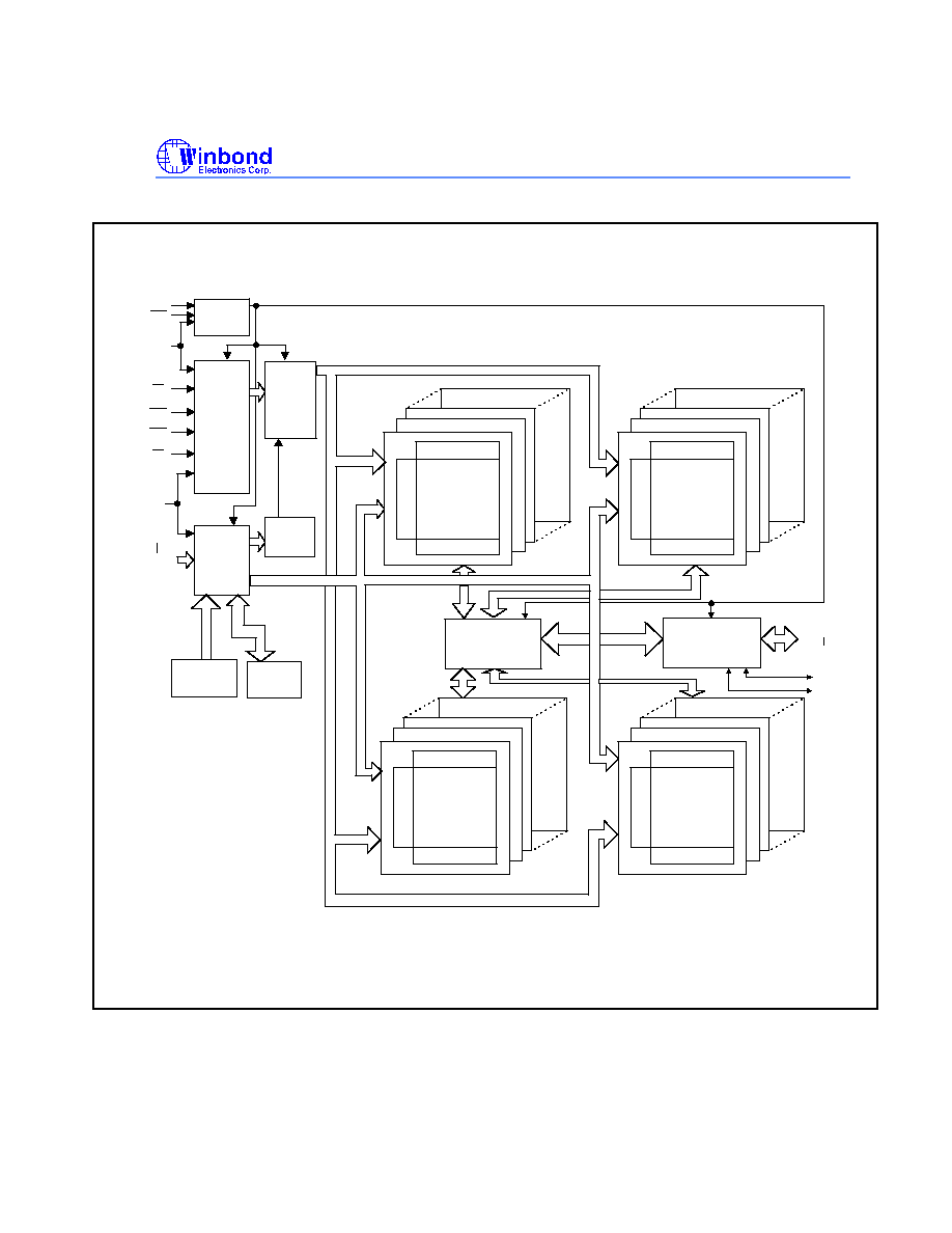
BLOCK DIAGRAM
DQS
CKE
A8
DLL
CLOCK
BUFFER
COMMAND
DECODER
ADDRESS
BUFFER
REFRESH
COUNTER
COLUMN
COUNTER
CONTROL
SIGNAL
GENERATOR
MODE
REGISTER
COLUMN DECODER
SENSE AMPLIFIER
CELL ARRAY
BANK #2
COLUMN DECODER
SENSE AMPLIFIER
CELL ARRAY
BANK #0
COLUMN DECODER
SENSE AMPLIFIER
CELL ARRAY
BANK #3
DATA CONTROL
CIRCUIT
DQ
BUFFER
COLUMN DECODER
SENSE AMPLIFIER
CELL ARRAY
BANK #1
NOTE:
The cell array configuration is 2048 * 256 * 32
ROW DECODER
ROW DECODER
ROW DECODER
ROW DECODER
A0
A7,
A9,A10
BA0
BA1
CS
RAS
CAS
WE
CLK
CLK
DM
DQ0
DQn
Prefetch Register
W946432AD
ABSOLUTE MAXIMUM RATINGS*
SYMBOL
ITEM
RATING
UNIT
NOTES
V
IN
Input Voltage
-0.3~ V
DD
+0.3
V
1
V
OUT
Output Voltage
-0.3~ V
DD
Q+0.3
V
1
V
DD
Power Supply Voltage
-0.3~4.6
V
1
V
DD
Q
I/O Power Supply Voltage
-0.3~3.6
V
1
T
OPR
Operating Temperature
0~70
°
C
1
T
STG
Storage Temperature
-55~150
°
C
1
T
SOLDER
Soldering Temperature(10s)
260
°
C
1
P
D
Power Dissipation
1
W
1
I
OUT
Short Circuit Output Current
50
mA
1
*
Conditions outside the limits listed under "Absolute Maxi-mum Ratings" may cause permanent damage to the device.
CAPACITANCE
(V
DD
Q = 2.5V, V
DD
= 2.5 ± 0.2, f 100 MHz, T
A
= 25 °C)
PARMETER
SYMBOL
MIN
MAX
UNITS
NOTES
Input Capacitance: CK, CK
Cl1
2.5
3.5
pF
Input Capacitance: All other input-only pins
Cl2
2.5
3.5
pF
Input/Output Capacitance: DQ, DQS, DM
Cl0
4.0
5.5
pF
Note: These parameters are periodically sampled and not 100% tested.
ELECTRICAL CHARACTERISTICS AND DC OPERATING CONDITIONS
(0°C
T
A
70°C; V
DD
Q = +2.5V ±0.2V, V
DD
= +2.5V ±0.2V
)
PARAMETER/CONDITION
SYMBOL
MIN
MAX
UNITS
NOTES
Supply Voltage (for devices with V
DD
of 2.5V)
V
DD
2.3
2.7
V
I/O Supply Voltage
V
DD
Q
2.3
2.7
V
I/O Reference Voltage
V
REF
1.15
1.35
V
3
I/O Termination Voltage (system)
V
TT
V
REF
-0.04
V
REF
+ 0.04
V
4
Input High (Logic 1) Voltage
V
IH
(
DC
)
V
REF
+0.18
V
DD
+ 0.3
V
Input Low (Logic 0) Voltage
V
IL
(
DC
)
-0.3
V
REF
-0.18
V
Input Voltage Level, CK and CK inputs
V
IN
(
DC
)
-0.3
V
DD
Q + 0.3
V
Input Differential Voltage, CK and CK inputs
V
ID
(
DC
)
0.36
V
DD
Q + 0.6
V
5
INPUT LEAKAGE CURRENT
Any input 0V
V
IN
V
DD
(All other pins not under test = 0V)
I
I
-5
5
uA
OUTPUT LEAKAGE CURRENT
(DQs are disabled; 0V
V
OUT
V
DD
Q)
I
OZ
-5
5
uA
OUTPUT LEVELS
Output High Current (V
OUT
= 1.95V)
I
OH
-15.2
m
A
Output Low Current (V
OUT
= 0.35V)
I
OL
15.2
m
A
W946432AD
AC OPERATING CONDITIONS
(0°C
T
A
70°C; V
DD
Q = +2.5V ± 0.2V, V
DD
= +2.5V ± 0.2V)
PARAMETER/CONDITION
SYMBOL
MIN
MAX
UNITS
NOTES
Input High (Logic 1) Voltage, DQ, DQS and DM signals
V
IH
(
AC
)
V
REF
+
0.35
V
Input Low (Logic 0) Voltage, DQ, DQS and DM signals
V
IL
(
AC
)
V
REF
-
0.35
V
Input Differential Voltage, CK and CK inputs
V
ID
(
AC
)
0.7
V
DD
Q + 0.6
V
5
Input Crossing Point Voltage, CK and CK inputs
V
IX
(
AC
)
0.5*V
DD
Q-0.2
0.5*V
DD
Q+0.2
V
7
I
DD
SPECIFICATIONS AND CONDITIONS
(0°C
T
A
70°C; V
DD
Q = +2.5V ± 0.2V, V
DD
= +2.5V ± 0.2V)
MAX
SYMBOL
UNITS
NOTES
OPERATING CURRENT: One Bank; Active-Precharge;
tRC = tRC MI
N;
tCK = tCK MIN; DQ, DM and DQS inputs changing twice per
clock cyle; address and control inputs changing once per clock cycle
I
DD
0
TBD
mA
OPERATING CURRENT: One Bank; Active-Read-Precharge;
Burst = 2; tRC = tRC MI
N;
CL = 3 ; tCK = tCK MIN; I
OUT
= 0 mA;
Address and control inputs changing once per clock cycle
I
DD
1
TBD
mA
PRECHARGE POWER-DOWN STANDBY CURRENT: All banks idle;
power-down mode; CKE
V
IL
(MAX); tCK = tCK MIN
I
DD
2P
TBD
mA
IDLE STANDBY CURRENT: CS
V
IH
(MIN); All banks idle;
CKE
V
IH
(MIN); tCK = tCK MIN; Address and other control inputs
changing once per clock cycle
I
DD
2N
TBD
mA
ACTIVE POWER-DOWN STANDBY CURRENT: One bank active;
power-down mode; CKE
V
IL
(MAX); tCK = tCK MIN
I
DD
3P
TBD
mA
ACTIVE STANDBY CURRENT: CS
V
IH
(MIN); CKE
V
IH
(MIN);
One bank; Active-Precharge; tRC = tRAS MA
X;
tCK = tCK MIN; DQ,
DM and DQS inputs changing twice per clock cycle; address and
other control inputs changing once per clock cycle
I
DD
3N
TBD
mA
OPERATING CURRENT: Burst = 2; Reads; Continuous burst;
One bank active; Address and control inputs changing once per clock
cycle; CL = 3 ; tCK = tCK MIN; I
OUT
= 0 mA
I
DD
4R
TBD
mA
OPERATING CURRENT: Burst = 2; Writes; Continuous burst;
One bank active; Address and control inputs changing once per clock
cycle; CL = 3 ; tCK = tCK MIN; DQ, DM and DQS inputs changing
twice per clock cycle
I
DD4W
TBD
mA
AUTO REFRESH CURRENT: tRC = tRFC (MI
N)
I
DD
5
TBD
mA
SELF REFRESH CURRENT: CKE
0.2V
I
DD
6
TBD
mA
W946432AD
512K
×
×
4 BANKS
×
×
32 BITS DDR SDRAM
PRELIMINARY DATA:9/8/00
7
AC CHARACTERISTICS
(0°C
TA
70°C; V
DD
Q = +2.5V ± 0.2V, V
DD
= +2.5V ± 0.2V)
PARAMETER
-4
-5
-6
UNIT
NOTE
MIN. MAX. MIN. MAX. MIN. MAX.
DQ output access time from CLK/ CLK
tAC
-0.1
0.1
-0.1
0.1
-0.1
0.1
tCK
DQS output access time from CLK/ CLK
tDQSCK
-0.1
0.1
-0.1
0.1
-0.1
0.1
tCK
CLK high-level width
tCH
0.45
0.55
0.45
0.55
0.45
0.55 tCK
CLK low-level width
tCL
0.45
0.55
0.45
0.55
0.45
0.55 tCK
Clock cycle time
tCLK
4
8
5
8
6
8
ns
8
DQ and DM input hold time
tDH
0.5
0.5
0.5
ns
DQ and DM input setup time
tDS
0.5
0.5
0.5
ns
DQ and DM input pulse width (for each input)
tDIPW
1
1.6
1.6
ns
Data-out high-impedance time from CLK/ CLK
tHZ
-0.1
0.1
tCK
Data-out low-impedance time from CLK/ CLK
tLZ
-0.1
0.1
tCK
DQS-DQ Skew (for DQS and associated DQ
signals)
tDQSQ
-0.5
0.5
-0.5
0.5
-0.5
0.5
ns
DQS-DQ Skew (for DQS and all DQ signals)
tDQSQA
-0.5
0.5
ns
DQ/DQS output valid time
tDV
0.35
0.35
0.35
tCK
Write command to first DQS latching transition
tDQSS
0.75
1.25
0.75
1.25
0.75
1.25 tCK
DQS input high pulse width
tDQSH
0.35
0.4
0.6
0.4
0.6
tCK
DQS input low pulse width
tDQSL
0.35
0.4
0.6
0.4
0.6
tCK
DQS falling edge to CLK setup time
tDSS
0.2
tCK
DQS falling edge hold time from CLK
tDSH
0.2
tCK
MODE REGISTER SET command cycle time
tMRD
2
tCK
Write postamble
tWPST
0.4
0.6
tCK
Write preamble
tWPRE
0.25
tCK
Address and Control input hold time
TIH
1
ns
Address and Control input setup time
TIS
1
ns
Read preamble
tRPRE
0.9
1.1
0.9
1.1
0.9
1.1
tCK
Read postamble
tRPST
0.4
0.6
tCK
ACTIVE to PRECHARGE command
tRAS
35
35
120K
42
120K ns
ACTIVE to ACTIVE/Auto Refresh command period
tRC
47
55
60
ns
Auto Refresh to Active/Auto Refresh command
period
tRFC
47
66
72
ns
ACTIVE to READ or WRITE delay
tRCD
3
15
18
tCK
PRECHARGE command period
tRP
3
15
18
tCK
ACTIVE bank A to ACTIVE bank B command
tRRD
2
11
12
tCK
Write recovery time
tWR
2
10
12
tCK
Auto Precharge write recovery + precharge time
tDAL
5
25
30
tCK
Internal Write to Read Command Delay
tWTR
2
tCK
9
Exit SELF REFRESH to non-READ command
tXSNR
47
ns
Exit SELF REFRESH to READ command
tXSRD
200
200
200
tCK
Average Periodic Refresh Interval
tREFI
15.6
15.6
15.6 us
W946432AD
512K
×
×
4 BANKS
×
×
32 BITS DDR SDRAM
PRELIMINARY DATA:9/8/00
8
NOTES
1. All voltages referenced to V
SS
.
2. Outputs measured with equivalent load:
R
T
=
25 ohms
VTT
A.C TEST LOAD
Rs = 25 ohms
30pF
3. V
REF
is expected to be equal to 0.5*V
DD
Q of the transmitting device, and to track variations in the DC level
of the same. Peak-to-peak noise on V
REF
may not exceed +/-2% of the DC value.
4. V
TT
is not applied directly to the device. V
TT
is a system supply for signal termination resistors, is expected
to be set equal to V
REF
, and must track variations in the DC level of V
REF
.
5. V
ID
is the magnitude of the difference between the input level on CK and the input level on CK .
6. I
DD
specifications are tested after the device is properly initialized.
7. VIX is the differential clock cross point voltage where input timing measurement is referenced.
CLK
CLK
VssQ
Vix
Vix
8. Beyond 8ns tCK, chip maybe in "DLL off" mode
9. WRITE interrupted by READ is not allowed.
Note:

W946432AD
9
FUNCTIONAL DESCRIPTION
The W946432AD is a high speed CMOS, dynamic random access memory containing 67,108,864 bits. The
W946432AD is internally configured as a quad bank DRAM.
The W946432AD uses a double data rate architecture to achieve high speed operation. The double data rate
architecture is essentially a 32 prefetch architecture, with an interface designed to transfer two data words
per clock cycle at the I/O pins. A single read or write access for the W946432AD consists of a single 32bit
wide, one clock cycle data transfer at the internal DRAM core and two corresponding 32bit wide, one half
clock cycle data transfers at the I/O pins.
Read and write accesses to the DDR SDRAM are burst oriented; accesses start at a selected location and
continue for a programmed number of locations in a programmed sequence. Accesses begin with the
registration of an ACTIVE command, which is then followed by a READ or WRITE command. The address
bits registered coincident with the ACTIVE command are used to select the bank and row to be accessed
(BA0, BA1 select the bank; A0-A10 select the row). The address bits registered coincident with the READ or
WRITE command are used to select the starting column location for the burst access.
Prior to normal operation, the DDR SDRAM must be initialized. The following sections provide etailed
information covering device initialization, register definition, command descriptions and device operation.
INITIALIZATION
W986432AD must be powered up and initialized in a predefined manner. Operational procedures other than
those specified may result in undefined operation. Power must first be applied to V
DD
, then to V
DD
Q, and
finally to V
REF
(and to the system V
TT
). V
TT
must be applied after V
DD
Q to avoid device latch up, which may
cause permanent damage to the device. V
REF
can be applied any time after V
DD
Q, but is expected to be
nominally coincident with V
TT
. Except for CKE, inputs are not recognized as valid until after V
REF
is applied.
CKE is an SSTL_2 input, but will detect an LVCMOS LOW level after V
DD
is applied. Maintaining an
LVCMOS LOW level on CKE during power up is required to guarantee that the DQ and DQS outputs will be
in the High-
Z
state, where they will remain until driven in normal operation (by a read access). After all power
supply and reference voltages are stable, and the clock is stable, the DDR SDRAM requires a 200µs delay
prior to applying an executable command.
Once the 200µs delay has been satisfied, a DESELECT or NOP command should be applied, and CKE
should be brought HIGH. Following the NOP command, a PRECHARGE ALL command should be applied.
Next a MODE REGISTER SET command should be issued for the Extended Mode Register, to enable the
DLL, then a MODE REGISTER SET command should be issued for the Mode Register, to reset the DLL,
and to program the operating parameters. 200 clock cycles are required between the DLL reset and any read
command. A PRECHARGE ALL command should be applied, placing the device in the "all banks idle" state.
Once in the idle state, two AUTO REFRESH cycles must be performed. Additionally, a MODE REGISTER
SET command for the Mode Register, with the reset DLL bit deactivated (i.e. to program operating
parameters without resetting the DLL) must be performed. Following these cycles, the DDR SDRAM is ready
for normal operation.

W946432AD
10
REGISTER DEFINITION
MODE REGISTER
The Mode Register is programmed by the MODE REGISTER SET command (MRS/EMRS)
when all banks
are idle and no bursts are in progress
.
The Mode Register is used to define the operation specific mode of of the DDR SDRAM. This definition
includes the selection of a burst length, a burst type, a CAS latency, and an operating mode, as shown in
Figure1:
The Extended Mode Register controls functions beyond those controlled by the Mode Register; these
additional functionsinclude DLL enable/disable,output drive strength selection. These functions as shown
inFigure1:.
Mode Register must be loaded, and the controller must wait the specified time before initiating the
subsequent operation. Violating either of these requirements will result in unspecified operation.
Figure1:Mode Register Definition
BA0
BA1
A10
A9
A8
A7
A6
A5
A4
A3
A2
A1
A0
12
10
9
8
7
6
5
4
3
2
1
0
0*
Extended Mode Register
Address Bus
BT
Operating Mode
0*
13
CAS Latency
Burst Latency
* BA0 and BA1
must be 0, 0 to select the
Mode Register (vs. the
Extended Mode Register).
A3
Burst Type
0
1
Burst Latency
Sequential
Interleaved
CAS Latency
Reserved
Reserved
Reserved
3
Reserved
A3 = 0
A3 = 1
Reserved
Reserved
2
2
4
4
8
8
Reserved
Reserved
Reserved
Reserved
Reserved
Reserved
Reserved
Reserved
A2 A1 A0
0 0 0
0 0 1
0 1 0
0 1 1
1 0 0
1 0 1
1 1 0
1 1 1
Operating Mode
Normal Operation
Normal Operation/Reset DLL
Vendor Specific Test Mode
All other states reserved
A6 A5 A4
0 0 0
0 0 1
0 1 0
0 1 1
1 0 0
1 0 1
1 1 0
1 1 1
A6-A0
Valid
VS
Valid
-
A7
A8
0
0
0
1
1
0
-
-
An-A9
0
0
0
-
VS = Vendor Specific
MODE REGISTER DEFINITION
Reserved
Reserved
Reserved
Enable
Disable
DS0
Normal
Weak (optional)
BA0 BA1 A10 A9
A8
A7
A6
A5
A4
A3
A2
A1
A0
12
11
10
9
8
7
6
5
4
3
2
1
0
1*
0*
DS1 DS0 DLL
A0
0
1
DLL
A1
0
1
* BA0 and BA1
must be 1, 0 to select the
Extended Mode Register (vs. the
base Mode Register).
Extended Mode Register
Address Bus
EXTENDED MODE REGISTER DEFINITION
DS2
Operating Mode
-
Valid
-
Operating Mode
Normal Operation
All other states reserved
A10-A4
A3-A0
0
A2
DS1
0
1
A3
DS2
0
1
W946432AD
11
Burst Length
Read and write accesses to the DDR SDRAM are burst oriented, with the burst length being programmable,
as shown in Table 1: The burst length determines the maximum number of column locations that can be
accessed for a given READ or WRITE command. Burst lengths of 2, 4, or 8 locations are available for both
the sequential and the interleaved burst types.
When a READ or WRITE command is issued, a block of columns equal to the burst length is effectively
selected. All accesses for that burst take place with in this block, meaning that the burst will wrap within the
block if a boundary is reached. The block is uniquely selected by A1-A7 when the burst length is set to two,
by A2-A7 when the burst length is set to four and by A3-A7 when the burst length is set to eight. The
remaining address bit is used to select the starting location within the block. The programmed burst length
applies to both READ and WRITE bursts.
Burst Type
Accesses within a given burst may be programmed to be either sequential or interleaved; this is referred to
as the burst type and is selected by bit A3.
The ordering of accesses within a burst is determined by the burst length, the burst type and the starting
column address, as shown in Table 1:.
Table 1:BURST DEFINITION
Order of Accesses Within a Burst
Burst Length
Starting Column
Address:
Type = Sequential
Type = Interleaved
A0
0
0 - 1
0 - 1
2
1
1 0
1 0
A1 A0
0 0
012-3
0-1-2-3
0 1
1230
1-0-3-2
1 0
2301
2-3-0-1
4
1 1
3012
3-2-1-0
A2 A1 A0
0 0 0
0-1-2-3-4-5-6-7
0-1-2-3-4-5-6-7
0 0 1
1-2-3-4-5-6-7-0
1-0-3-2-5-4-7-6
0 1 0
2-3-4-5-6-7-0-1
2-3-0-1-6-7-4-5
0 1 1
3-4-5-6-7-0-1-2
3-2-1-0-7-6-5-4
1 0 0
4-5-6-7-0-1-2-3
4-5-6-7-0-1-2-3
1 0 1
5-6-7-0-1-2-3-4
5-4-7-6-1-0-3-2
1 1 0
6-7-0-1-2-3-4-5
6-7-4-5-2-3-0-1
8
1 1 1
7-0-1-2-3-4-5-6
7-6-5-4-3-2-1-0
NOTE:
1. For a burst length of two, A1-A7 selects the two-data-element block; A0 selects
the first access within the block.
2. For a burst length of four, A2-A7 selects the four-data-element block; A0-A1
selects the first access within the block.
3. For a burst length of eight, A3-A7 selects the eight-data- element block; A0-A2
selects the first access within the block.
4. Whenever a boundary of the block is reached within a given sequence above, the
following access wraps within the block.
W946432AD
12
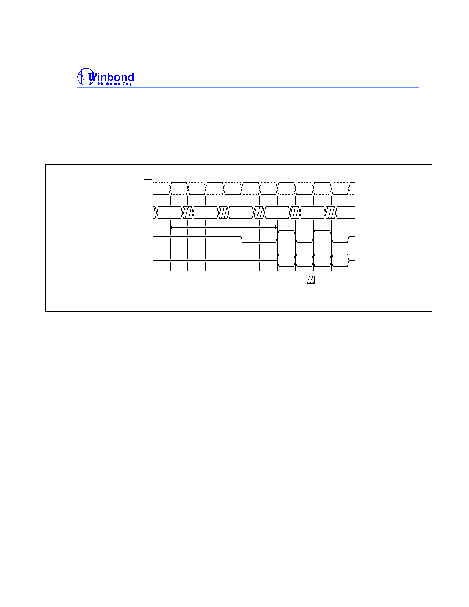
Read Latency
The READ latency is the delay, in clock cycles, between the registration of a READ command and the
availability of the first piece of output data. The latency is set to 3 clocks.
If a READ command is registered at clock edge n, and the latency is 3 clocks, the data will be available
nominally coincident with clock edge n + 3.
Figure2:REQUIRED CAS LATENCIES
NOP
NOP
READ
NOP
NOP
NOP
COMMAND
CK
CK
DQS
DQ
DON'T CARE
REQUIRED CAS LATENCIES
CL=3
Burst Length = 4 in the case shown
Shown with nominal tAC, tDQSCK, and tDQSQ
Operating Mode
The normal operating mode is selected by issuing a Mode Register Set command with bits A7-A10 each set
to zero, and bits A0-A6 set to the desired values. A DLL reset is inititated by issuing a Mode Register Set
command with bits A7 and A9-A10 each set to zero, bit A8 set to one, and bits A0-A6 set to the desired
values. A Mode Register Set command issued to reset the DLL should always be followed by a Mode
Register Set command to select normal operating mode.
All other combinations of values for A7-A10 are reserved for future use and/or test modes. Test modes and
reserved states should not be used because unknown operation or incompatibility with future versions may
result.
DLL Enable/Disable
The DLL must be enabled for normal operation. DLL enable isrequiredduringpower-upinitialization,andupon
returning to normal operation after having disabled the DLL for the purpose of debug or evaluation (upon
exiting Self Refresh Mode, the DLL is enabled automatically). Any time the DLL is enabled, 200 clock cycles
must occur before a READ command can be issued.
Output Drive Strength
DS0, DS1, DS2,
TBD
W946432AD
13
COMMANDS
Truth Table provides a quick reference of available commands. This is followed by a verbal description of
each command. The additional Function Truth Tables provide current state/ next state information.
TRUTH TABLE (NOTE 1, 2)
Symbol
Command
Device
State
CKEn-1 CKEn
DM BA0,1 A8
A10,
A9-0
CS RAS
CAS
WE
ACT
Bank Active
Idle (3)
H
X
X
V
V
V
L
L
H
H
PRE
Bank Precharge
Any (3)
H
X
X
V
L
X
L
L
H
L
PREA
Precharge All
Any
H
X
X
X
H
X
L
L
H
L
WRIT
Write
Active (3)
H
X
X
V
L
V
L
H
L
L
WRITA Write with Autoprecharge
Active (3)
H
X
X
V
H
V
L
H
L
L
READ
Read
Active (3)
H
X
X
V
L
V
L
H
L
H
READA Read with Autoprecharge
Active (3)
H
X
X
V
H
V
L
H
L
H
MRS
Mode Register Set
Idle
H
X
X
L,L
V
V
L
L
L
L
EMRS
Extended Mode Register Set
H
X
X
H,L
V
V
L
L
L
L
NOP
No-Operation
Any
H
X
X
X
X
X
L
H
H
H
BST
Burst Read Stop
Active (4)
H
X
X
X
X
X
L
H
H
L
DSL
Device Deselect
Any
H
X
X
X
X
X
H
X
X
X
AREF
Auto-Refresh
Idle
H
H
X
X
X
X
L
L
L
H
SELF
Self-Refresh Entry
Idle
H
L
X
X
X
X
L
L
L
H
SELEX Self-Refresh Exit
Idle
(S.R)
L
H
X
X
X
X
H
L
X
H
X
H
X
X
PD
Power Down Mode Entry
Idle
Active (5)
H
L
X
X
X
X
H
L
X
H
X
H
X
X
PDEX
Power Down Mode Exit
Any
(Power down)
L
H
X
X
X
X
H
L
X
H
X
H
X
X
WDE
Data Write Enable
Active
H
X
L
X
X
X
X
X
X
X
WDD
Data Write Disable
Active
H
X
H
X
X
X
X
X
X
X
Notes:
(1) V = Valid, X = Don't care, L = Low Level, H = High Level
(2) CKEn signal is input level when commands are provided.
CKEn-1 signal is input level one clock cycle before the command provided.
(3) These are state of bank designated by BA0 BA1 signals.
(4) Applies only to read bursts with autoprecharge disabled; this command should not be used for read
bursts with autoprecharge enabled, and for write bursts.
(5) Power Down Mode can not be entered in the burst cycle.
W946432AD
14
Function TRUTH TABLE (NOTE 1)
CURRENT
STATE
CS RAS CAS WE Address Command
ACTION
NOTE
H
X
X
X
X
DSL
NOP
L
H
H
X
X
NOP, BST NOP
L
H
L
H
BA, CA,A8 Read, Read A ILLEGAL
3
L
H
L
L
BA, CA,A8 Write, Write A ILLEGAL
3
L
L
H
H
BA, RA
ACT
ACTIVE (select and activate row)
L
L
H
L
BA, A8
PRE, PRE A NOP
L
L
L
H
X
AREF, SREF Refresh or Self refresh
2
Idle
L
L
L
L
Op-Code MRS, EMRS Mode register accessing
2
H
X
X
X
X
DSL
NOP
L
H
H
X
X
NOP, BST NOP
L
H
L
H
BA, CA,A8 Read, Read A READ (start READ burst)
4
L
H
L
L
BA, CA,A8 Write, Write A WRITE (start WRITE burst)
4
L
L
H
H
BA, RA
ACT
ILLEGAL
3
L
L
H
L
BA, A8
PRE, PRE A PRECHARGE
5
L
L
L
H
X
AREF, SREF ILLEGAL
Row Active
L
L
L
L
Op-Code MRS, EMRS ILLEGAL
H
X
X
X
X
DSL
Continue burst to end
L
H
H
H
X
NOP
Continue burst to end
L
H
H
L
X
BST
Burst stop
L
H
L
H
BA, CA,A8 Read, Read A Term burst, start new READ burst
6
L
H
L
L
BA, CA,A8 Write, Write A ILLEGAL
L
L
H
H
BA, RA
ACT
ILLEGAL
3
L
L
H
L
BA, A8
PRE, PRE A Term burst, PRECHARGE
L
L
L
H
X
AREF, SREF ILLEGAL
Read
L
L
L
L
Op-Code MRS, EMRS ILLEGAL
H
X
X
X
X
DSL
Continue burst to end
L
H
H
H
X
NOP
Continue burst to end
L
H
H
L
X
BST
ILLEGAL
L
H
L
H
BA, CA,A8 Read, Read A ILLEGAL
3
L
H
L
L
BA, CA,A8 Write, Write A Term burst, start new READ burst
6,7
L
L
H
H
BA, RA
ACT
ILLEGAL
3
L
L
H
L
BA, A8
PRE, PRE A Term burst, PRECHARGE
L
L
L
H
X
AREF, SREF ILLEGAL
8
Write
L
L
L
L
Op-Code MRS, EMRS ILLEGAL
H
X
X
X
X
DSL
Continue burst to end
L
H
H
H
X
NOP
Continue burst to end
L
H
H
L
X
BST
ILLEGAL
L
H
L
H
BA, CA,A8 Read, Read A ILLEGAL
L
H
L
L
BA, CA,A8 Write, Write A ILLEGAL
L
L
H
H
BA, RA
ACT
ILLEGAL
L
L
H
L
BA, A8
PRE, PRE A ILLEGAL
L
L
L
H
X
AREF, SREF ILLEGAL
Read with
Auto
rpecharge
L
L
L
L
Op-Code MRS, EMRS ILLEGAL
H
X
X
X
X
DSL
Continue burst to end
L
H
H
H
X
NOP
Continue burst to end
L
H
H
L
X
BST
ILLEGAL
L
H
L
H
BA, CA,A8 Read, Read A ILLEGAL
L
H
L
L
BA, CA,A8 Write, Write A ILLEGAL
L
L
H
H
BA, RA
ACT
ILLEGAL
L
L
H
L
BA, A8
PRE, PRE A ILLEGAL
L
L
L
H
X
AREF, SREF ILLEGAL
Write with
Auto
precharge
L
L
L
L
Op-Code MRS, EMRS ILLEGAL
W946432AD
15
NOTE:
1. This table applies when CKE n-1 was HIGH and CKE n is HIGH.
2. ILLEGAL if any bank is not idle.
3. ILLEGAL to bank in specified states; Function may be legal in the bank indicated by Bank Address(BA), depending on the state of
that bank.
4. ILLEGAL if tRCD is not satisfied.
5. ILLEGAL if tRAS is not satisfied.
6. Must satisfy bust interrupt condition.
7. Must satisfy bus contention, bus turn around, and/ or write recovery requirements
8. Must mask preceding data, which don't satisfy tWR
Figure3:Simplified State Diagram
SIMPLIFIED STATE DIAGRAM
POWER
APPLIED
Automatic Sequence
Command Sequence
Read A
Write
Read
ROW
ACTIVE
POWER
DOWN
IDLE
MODE
REGISTER
SET
AUTO
REFRESH
SELF
REFRESH
Read
Read A
Write
Write A
PRE
CHARGE
POWER
ON
MRS/EMRS
AREF
SREF
SREFX
PD
PDEX
ACT
BST
Read
Write
Write A
Write A
Read A
PRE
PRE
PRE
PRE
ACTIVE
POWERDOWN
PD
PDEX
MRS = Mode Register Set
EMRS = Extended Mode Register Set
SREF = Enter Self Refresh
SREFX = Exit Self Refresh
AREF = Auto Refresh
PD = Enter Power Down
PDEX = Exit Power Down
ACT = Active
Write A = Write with Autoprecharge
Read A = Read with Autoprecharge
PRE = Precharge
BST = B nst Read Stpop

W946432AD
16
DESELECT
The Device Deselect command disables the command decoder so that the
RAS
CAS
WE
and Address
inputs are ignored. This command is similar to the No-Operation command.
NO OPERATION (NOP)
The No Operation Command should be used in cases when the DDR SDRAM is in an idle or a wait state to
prevent the DDR SDRAM from registering any unwanted commands between operations. A No Operation
Command is registered when
CS
is low with
RAS
,
CAS
, and
WE
held high at the rising edge of the clock.
A No Operation Command will not terminate a previous operation that is still executing, such as a burst read
or write cycle.
MODE REGISTER SET
Command is registered when
CS
,
RAS
,
CAS
, and
WE
is at the rising edge of the clock. The mode
registers are loaded by inputs A0-A10. See mode register descriptions in the Register Definition section. The
MODE REGISTER SET command can only be issued when all banks are idle and no bursts are in progress,
and a subsequent executable command cannot be issued until tMRD is met.
ACTIVE
The ACTIVE command is registered when
CS
,
RAS
is low with
CAS
, and
WE
held high at the rising edge
of the clock, used to open a row in a particular bank for a subsequent access.
READ
The READ command is registered when
CS
,
CAS
is low with
RAS
, and
WE
held high at the rising edge of
the clock, used to initiate a burst read access to an active row. The value on the BA0, BA1 inputs selects the
bank, and the address provided on inputs A0-A7 selects the starting column location.
WRITE
The WRITE command is registered when
CS
,
CAS
,
WE
is low with
RAS
, held high at the rising edge of
the clock, used to initiate a burst write access to an active row. The value on the BA0, BA1 inputs selects the
bank, and the address provided on inputs A0-A7 selects the starting column location
PRECHARGE
The PRECHARGE command is registered when
CS
,
RAS
,
WE
is low with
CAS
held high at the rising
edge of the clock, used to deactivate the open row in a particular bank or the open row in all banks. The
bank(s) will be available for a subsequent row access a specified time ( tRP) after the PRECHARGE
command is issued. Input A8 determines whether one or all banks are to be precharged, and in the case
where only one bank is to be precharged, inputs BA0, BA1 select the bank. When all banks are to be
precharged, inputs BA0, BA1 are treated as "Don't Care." Once a bank has been precharged, it is in the idle
state and must be activated prior to any READ or WRITE commands being issued to that bank. A
PRECHARGE command will be treated as a NOP if there is no open row in that bank.
BURST READ STOP
The BURST READ STOP command register when
CS
WE
is low with RAS CAS held high is used to
truncate read bursts (with autoprecharge disabled).
AUTO REFRESH
The Auto Refresh command is register when
CS
RAS
CAS
low with
WE
high.
The refresh addressing is generated by the internal refresh controller. This makes the address bits "Don't
Care" during an AUTO REFRESH command. The W946432AD requires AUTO REFRESH cycles at an
average periodic interval of 15.6µs (maximum).

W946432AD
PRELIMINARY DATE: 9/8/00
17 .
To allow for improved efficiency in scheduling and switching between tasks, some flexibility in the absolute
refresh interval is provided. A maximum of eight AUTO REFRESH commands can be posted to any given
DDR SDRAM, meaning that the maximum absolute interval between any AUTO REFRESH command and
the next AUTO REFRESH command is 9 * 15.6us (140.4us). This maximum absolute interval is short
enough to allow for DLL updates internal to the DDR SDRAM to be restricted to AUTO REFRESH cycles,
without allowing too much drift in tAC between updates.
SELF REFRESH
The SELF REFRESH command can be used to retain data in the DDR SDRAM, even if the rest of the
system is powered down. When in the self refresh mode, the DDR SDRAM retains data without external
clocking. The SELF REFRESH command is initiated like an AUTO REFRESH command except CKE is
disabled (LOW). The DLL is automatically disabled upon entering SELF REFRESH, and is automatically
enabled upon exiting SELF REFRESH (200 clock cycles must then occur before a READ command can be
issued). Input signals except CKE are "Don't Care" during SELF REFRESH.
The procedure for exiting self refresh requires a sequence of commands. First, CK must be stable prior to
CKE going back HIGH. Once CKE is HIGH, the DDR SDRAM must have NOP commands issued for tXSNR
because time is required for the completion of any internal refresh in progress. A simple algorithm for
meeting both refresh and DLL requirements is to apply NOPs for 200 clock cycles before applying any other
command.
OPERATIONS
BANK/ROW ACTIVATION
Before any READ or WRITE commands can be issued to a bank within the DDR SDRAM, a row in that bank
must be "opened." This is accomplished by the ACTIVE command, which selects both the bank and the row
to be activated.
The value on the BA0, BA1 inputs selects the bank, and the address provided on inputs A0-A10 selects the
row. The maximum time that each bank can be held in the active state is specified as tRAS (max). After this
command is issued, Read or Write operation can be executed.
After opening a row, a READ or WRITE command may be issued to that row, subject to the tRCD
specification.
A subsequent ACTIVE command to a different row in the same bank can only be issued after the previous
active row has been "closed" (precharged). The minimum time interval between successive ACTIVE
commands to the same bank is defined by tRC.
A subsequent ACTIVE command to another bank can be issued while the first bank is being accessed, which
results in a reduction of total row access overhead. The minimum time interval between successive ACTIVE
commands to different banks is defined by tRRD.
W946432AD
PRELIMINARY DATE: 9/8/00
18 .
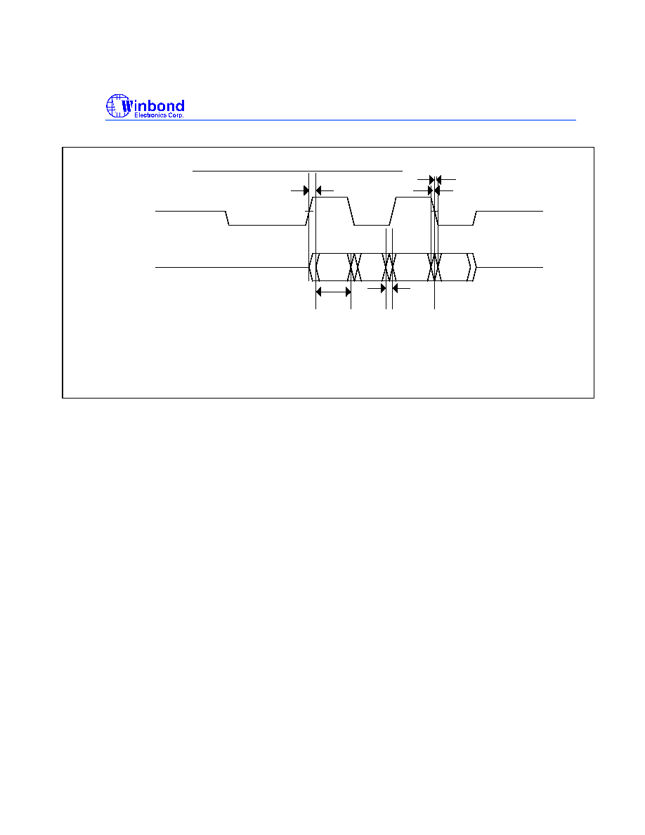
Figure4:tRCD and tRRD Definition
CK
CK
NOP
ACT
Row
Col
Row
Bank x
Bank y
Bank y
tRRD
tRCD
COMMAND
A0-A10
BA0,BA1
tRCD and tRRD Definition
DON'T CARE
NOP
NOP
ACT
NOP
NOP
RD/WR
READs
The starting column and bank addresses are provided with the READ command and AUTO PRECHARGE is
either enabled or disabled for that burst access. If AUTO PRECHARGE is enabled (A8 = high), the row that
is accessed will start precharge at the completion of the burst. This command cannot be interrupted by any
other command. For the generic READ commands used in the following illustrations, AUTO PRECHARGE is
disabled (A8 = low).
During READ bursts, the valid data-out element from the starting column address will be available following
the CAS latency after the READ command. Each subsequent data-out element will be valid nominally at the
next positive or negative clock edge. Figure5: shows general timing. DQS is driven by the DDR SDRAM
along with output data. The initial LOW state on DQS is known as the read preamble; the LOW state
coincident with the last data-out element is known as the read post amble. Upon completion of a burst,
assuming no other commands have been initiated, the DQS will go High-Z.
Data from any READ burst may be concatenated with or truncated with data from a subsequent READ
command. In either case, a continuous flow of data can be maintained. The first data element from the new
burst follows either the last element of a completed burst or the last desired data element of a longer burst
which is being truncated. The new READ command should be issued
x cycles after the first READ
command, where
x equals the number of desired data element pairs (pairs are required by the 32 prefects
architecture). This is shown in Figure6:. A READ command can be initiated on any clock cycle following a
previous READ command. Non-consecutive READ data is shown for illustration in Figure7:. Full-speed
random read accesses within a page (or pages) can be performed as shown in Figure8:.
Data from any READ burst may be truncated with a BURST READ STOP command, as shown in
Figure9:The BURST READ STOP latency is equal to the read ( CAS ) latency.
Data from any READ burst must be completed or truncated before a subsequent WRITE command can be
issued. If truncation is necessary, the BURST READ STOP command must be used, as shown in Figure10:.
A READ burst may be followed by, or truncated with, a PRECHARGE command to the same bank (provided
that AUTO PRECHARGE was not activated). The PRECHARGE command should be issued
x cycles after
the READ command, where
x equals the number of desired data element pairs. Note that part of the row
precharge time is hidden during the access of the last data elements.
W946432AD
PRELIMINARY DATE: 9/8/00
19 .
In the case of a READ being executed to completion, a PRECHARGE command issued at the optimum time
(as described above) provides the same operation that would result from the same READ burst with AUTO
PRECHARGE enabled. The disadvantage of the PRECHARGE command is that it requires that the
command and address buses be available at the appropriate time to issue the command. The advantage of
the PRECHARGE command is that it can be used to truncate bursts.
Figure5:READ BURST REQUIRED CAS LATENCIES
NOP
NOP
READ
NOP
NOP
NOP
COMMAND
CK
CK
DQS
DQ
DON'T CARE
Bank,
READ BURST - REQUIRED CAS LATENCIES
ADDRESS
CL=3
Col n
DO
n
DO n = Data Out from column n
Burst Length = 4
Show with nominal tAC, tDQSCK, and tDQSQ
W946432AD
PRELIMINARY DATE: 9/8/00
20 .
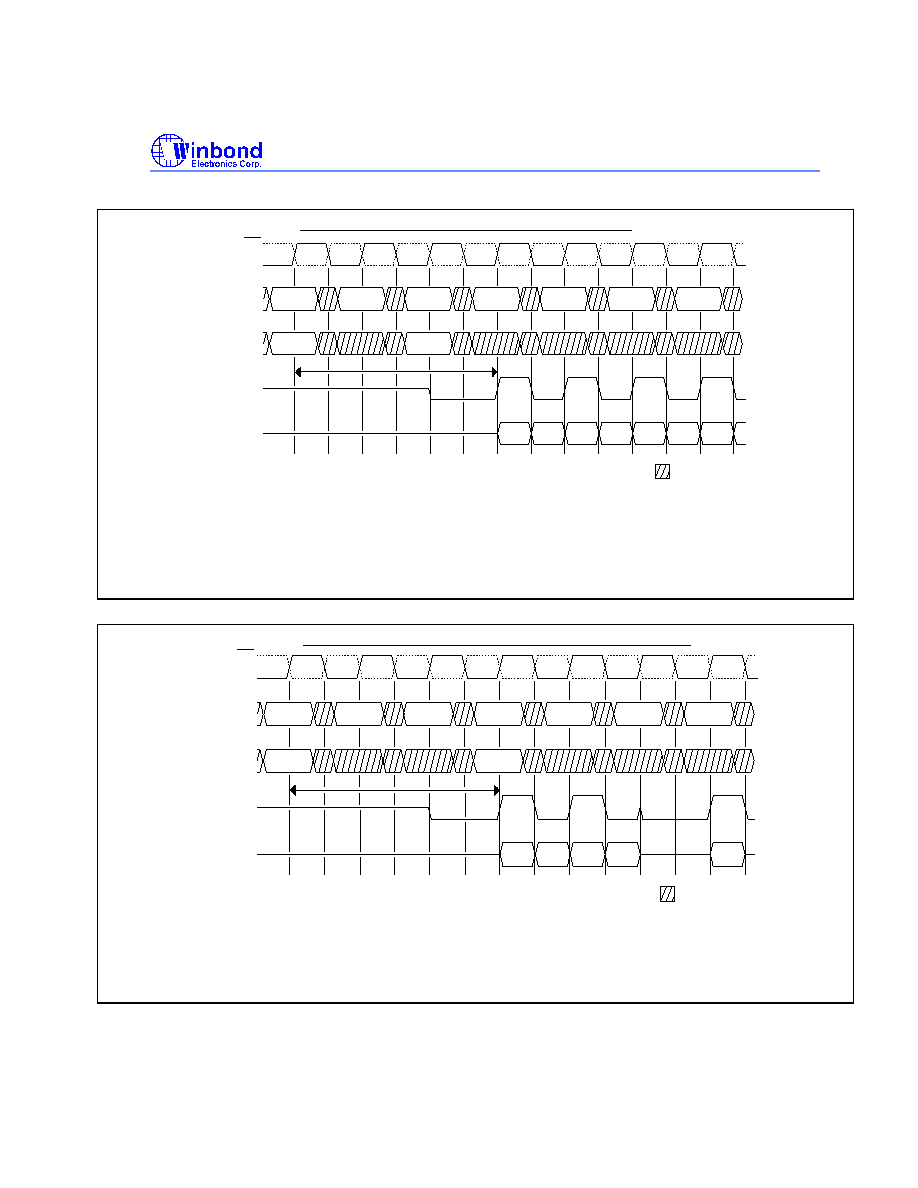
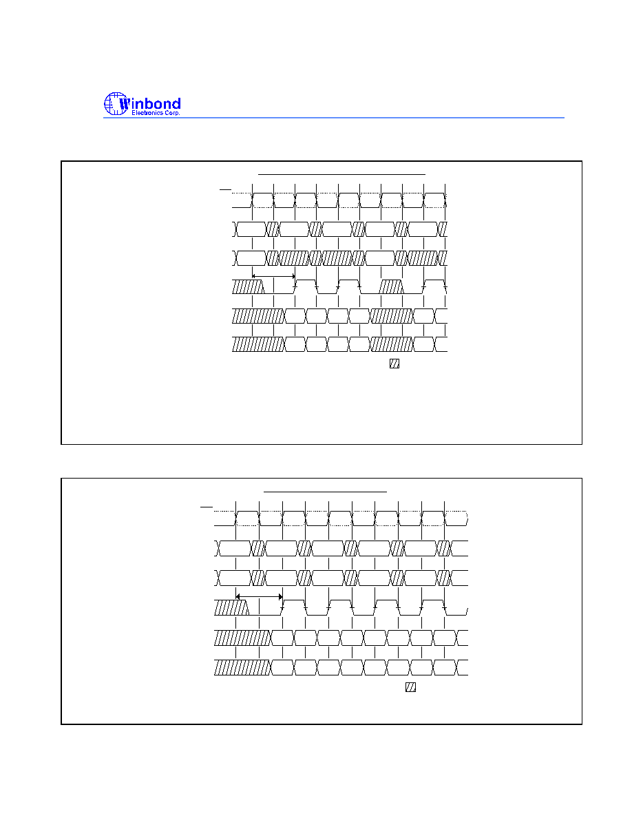
Figure6:CONSECUTIVE READ BURSTS REQUIRED CAS LATENCIES
NOP
READ
NOP
NOP
NOP
COMMAND
CK
CK
DQS
DQ
DON'T CARE
Bank,
CONSECUTIVE READ BURSTS - REQUIRED CAS LATENCIES
ADDRESS
CL=3
Col n
NOP
DO
n
DO
b
Bank,
Col n
READ
DO n (or b) = Data Out from column n (or column b)
Burst Length = 4
Shown with nominal tAC, tDQSCK, and tDQSQ
Read commands shown must be to the same device
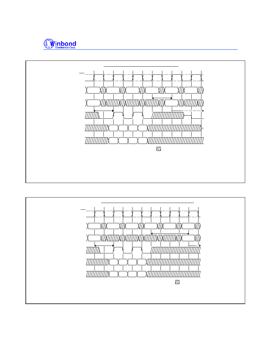
Figure7:NON CONSECUTIVE READ BURSTS REQUIRED CAS LATENCIES
NOP
NOP
READ
NOP
NOP
COMMAND
CK
CK
DQS
DQ
DON'T CARE
Bank,
NON CONSECUTIVE READ BURSTS - REQUIRED CAS LATENCIES
ADDRESS
CL=3
Col n
DO
n
NOP
READ
Bank,
Col b
DO
b
DO n (or b) = Data Out from column n (or column b)
Burst Length = 4
Shown with nominal tAC, tDQSCK, and tDQSQ
W946432AD
21
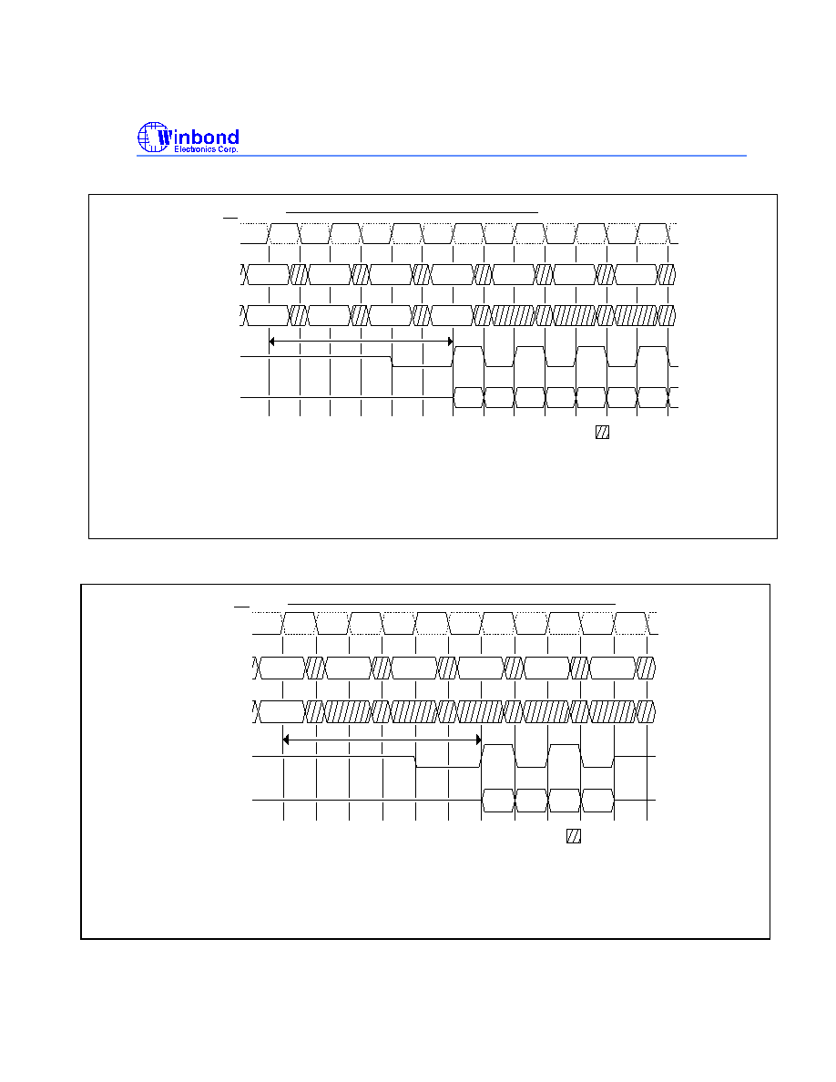
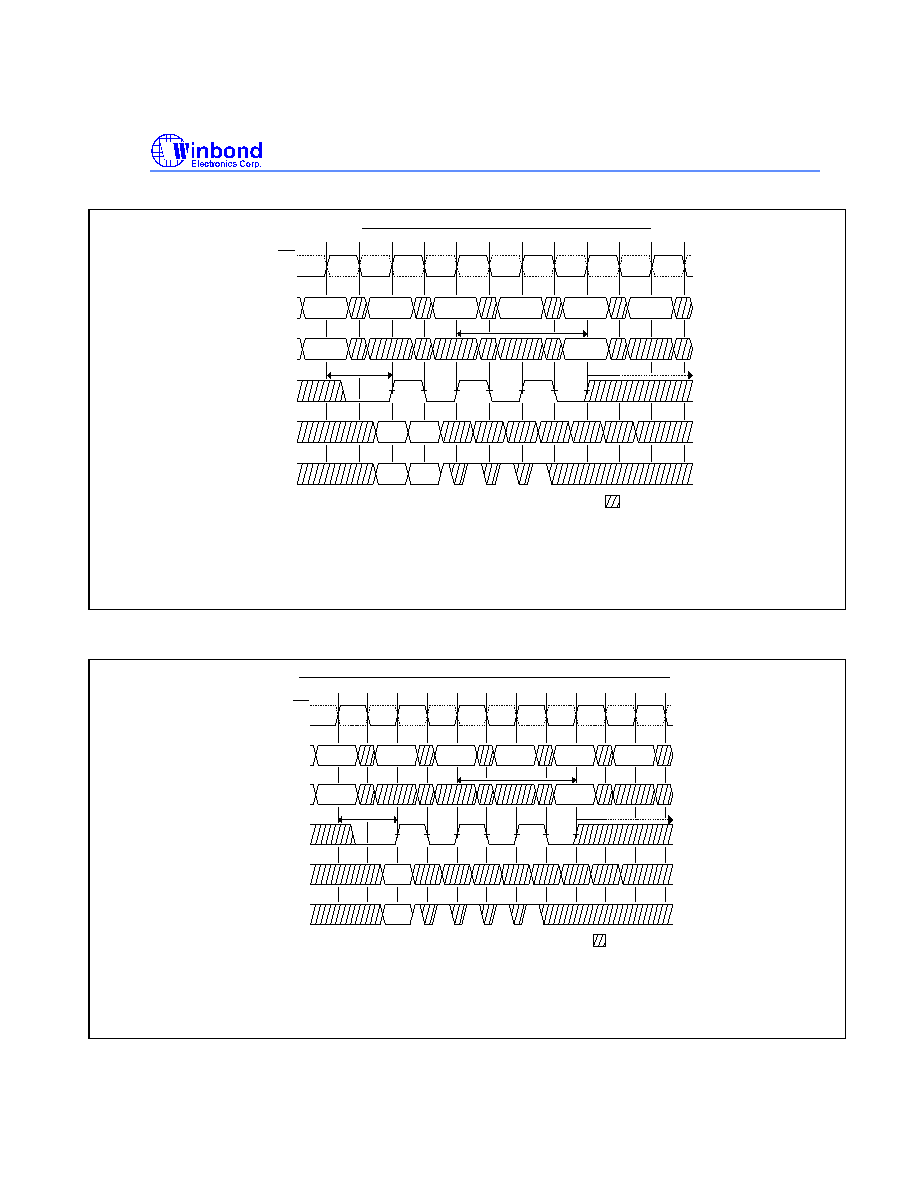
Figure8:RANDOM READ ACCESSES REQUIRED CAS LATENCIES
READ
NOP
COMMAND
CK
CK
DQS
DQ
DON'T CARE
Bank,
RANDOM READ ACCESSES - REQUIRED CAS LATENCIES
ADDRESS
CL=3
Col n
NOP
DO
n
DO
b
Bank,
Col b
READ
READ
READ
READ
Bank,
Col x
Bank,
Col g
DO
n'
DO
x
DO
x'
DO
g
DO
b'
DO n, etc. = Data Out from column n, etc.
n', etc. = the next Data Out following DO n, etc. according to the programmed burst order
Burst Length = 4
Reads are to active rows in any banks
Shown with nominal tAC, tDQSCK, and tDQSQ
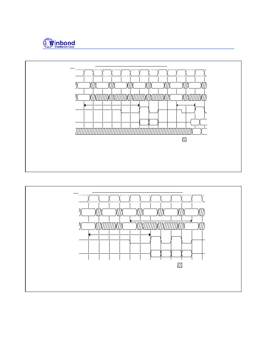
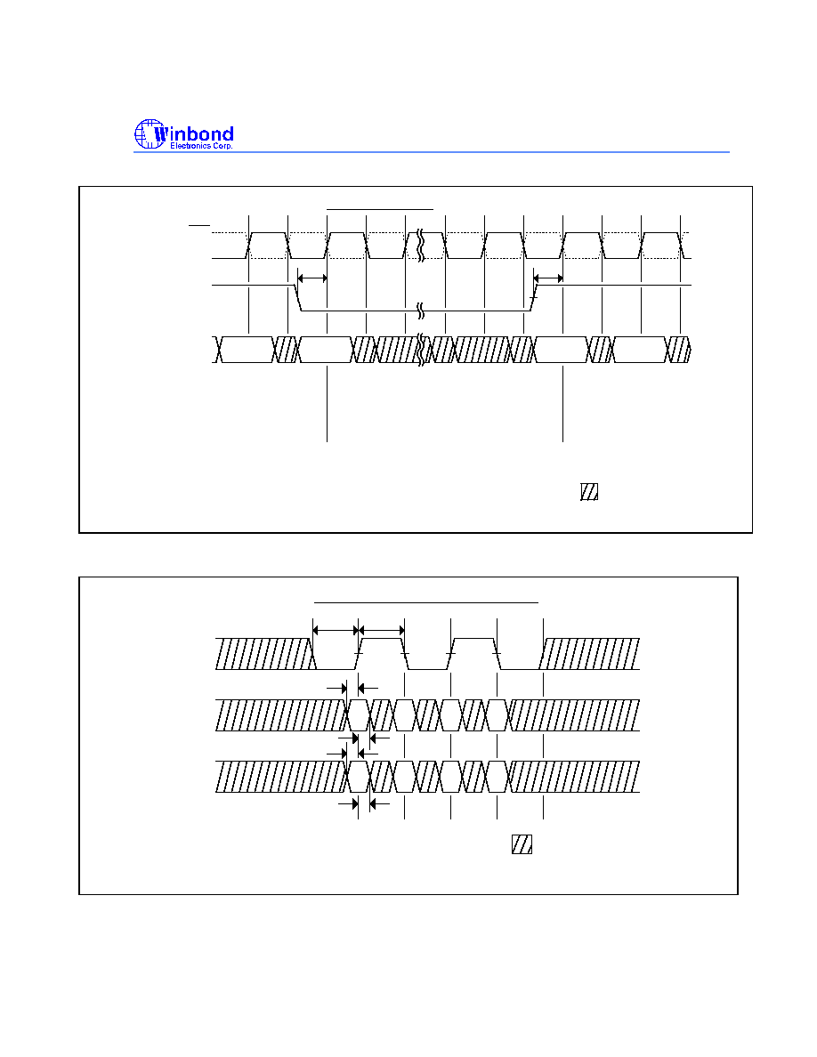
Figure9:BURST READ STOP REQUIRED CAS LATENCIES
NOP
BST
READ
NOP
NOP
NOP
COMMAND
CK
CK
DQS
DQ
DON'T CARE
Bank,
TERMINATING A READ BURST - REQUIRED CAS LATENCIES
ADDRESS
CL=3
Col n
DO
n
DO n = Data Out from column n
Cases shown are bursts of 8 terminated after 4 data elements
Shown with nominal tAC, tDQSCK, and tDQSQ
W946432AD
22
Figure10:READ TO WRITE REQUIRED CAS LATENCIES
BST
NOP
READ
NOP
NOP
COMMAND
CK
CK
DQS
DQ
Bank,
READ TO WRITE - REQUIRED CAS LATENCIES
ADDRESS
CL=3
Col n
DO
n
WRITE
Bank,
Col b
NOP
t
DQSS
DON'T CARE
DM
DO n (or b) = Data Out from column n (or column b)
Burst Length = 4
Data In elements are applied following DI b in the programmed order
Shown with nominal tAC, tDQSCK, and tDQSQ
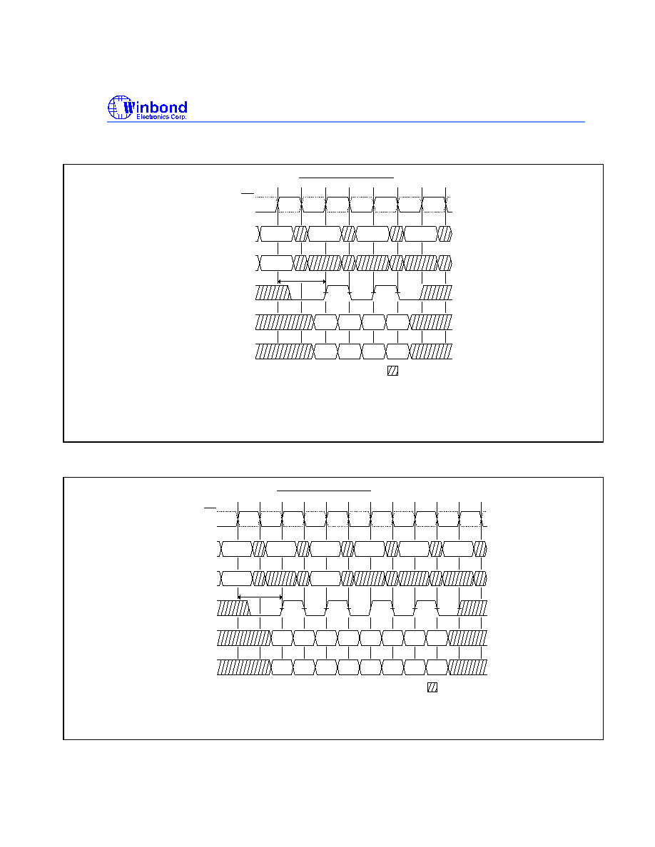
Figure11:READ TO PRECHARGE REQUIRED CAS LATENCIES
NOP
READ
NOP
NOP
ACT
COMMAND
CK
CK
DQS
DQ
DON'T CARE
Bank,
READ TO PRECHARGE - REQUIRED CAS LATENCIES
ADDRESS
CL=3
Col n
DO
n
Bank
(a or all)
PRE
Bank,
Row
t
RP
DO n (or b) = Data Out from column n Cases shown are either uninterrupted bursts of 4, or interrupted bursts of 8
Shown with nominal tAC, tDQSCK, and tDQSQ

W946432AD
23
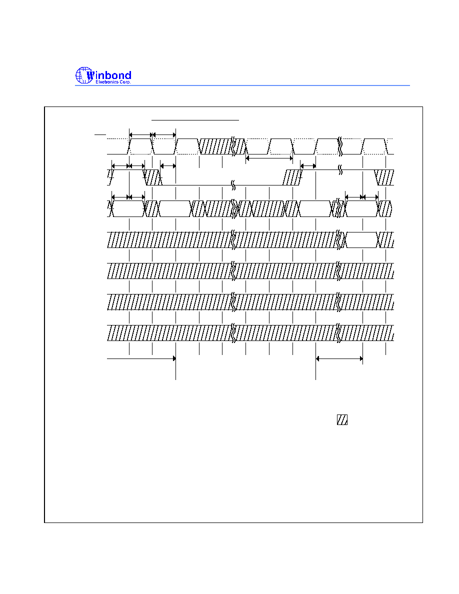
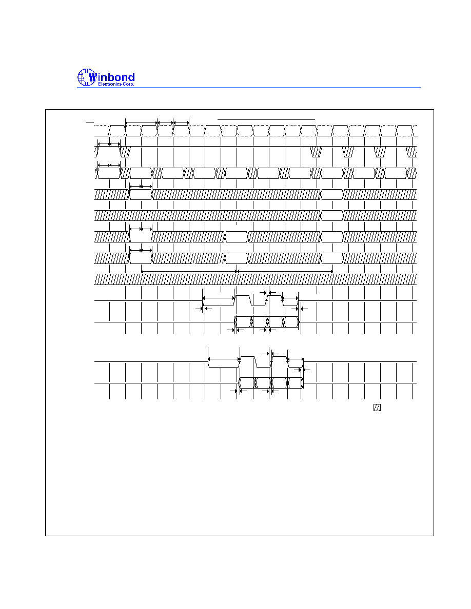
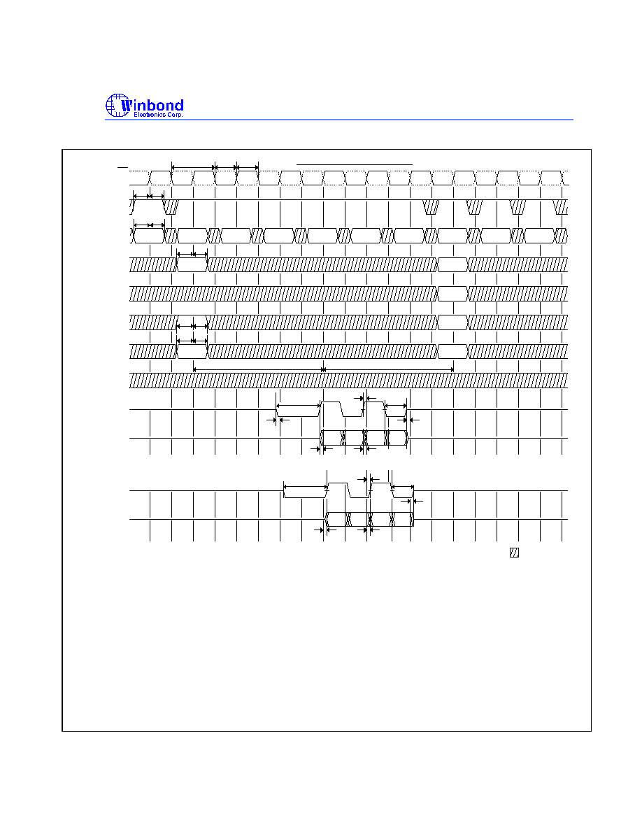
WRITEs
The starting column and bank addresses are provided with the WRITE command, and AUTO PRECHARGE
is either enabled or disabled for that access. If AUTO PRECHARGE is enabled (A8=HIGH), the row being
accessed will be precharged at the end of the WRITE burst; if AUTO PRECHARGE is disabled (A8=LOW),
the row will remain open for subsequent accesses.
During WRITE bursts, the first valid data-in element will be registered on the first rising edge of DQS
following the write command, and subsequent data elements will be registered on successive edges of DQS.
The LOW state on DQS between the WRITE command and the first rising edge is known as the write
preamble; the LOW state on DQS following the last data-in element is known as the write post amble. The
time between the WRITE command and the first corresponding rising edge of DQS (tDQSS) is specified with
a relatively wide range (from 75% to 125% of 1 clock cycle), Figure12: show the two extremes of tDQSS for a
burst of 4. Upon completion of a burst, assuming no other commands have been initiated, the DQS will
remain High-Z and any additional input data will be ignored.
Data for any WRITE burst may be concatenated with or truncated with a subsequent WRITE command. In
either case, a continuous flow of input data can be maintained. The new WRITE command can be issued on
any positive edge of clock following the previous WRITE command. The first data element from the new
burst is applied after either the last element of a completed burst or the last desired data element of a longer
burst, which is being truncated. The new WRITE command should be issued
x cycles after the first WRITE
command, where
x equals the number of desired data element pairs Figure13: show concatenated bursts of
4. An example of non-consecutive WRITEs is shown in. 0 Full-speed random write accesses within a page or
pages can be performed as shown in. Figure15: Data for any WRITE burst may be followed by a subsequent
READ command. To follow a WRITE without truncating the write burst, tWTR should be met as shown in
Figure16:.
Data for any WRITE burst may be followed by a subsequent PRECHARGE command. To follow a WRITE
without truncating the write burst, tWR should be met as shown in 0.
Data for any WRITE burst may be truncated by a subsequent PRECHARGE command, as shown in
Figure18: Figure19:. Note that only the data-in pairs that are registered prior to the tWR period are written to
the internal array, and any subsequent data-in should be masked with DM, as shown in Figure18: Figure19:.
Following the PRECHARGE command, a subsequent command to the same bank cannot be issued until t
RP is met.
POWER-DOWN
Power-down is entered when CKE is registered LOW (no accesses can be in progress). If power-down
occurs when all banks are idle, this mode is referred to as precharge power-down; if power-down occurs
when there is a row active in any bank, this mode is referred to as active power-down. Entering power-down
deactivates the input and output buffers, excluding CK, CK and CKE. For maximum power savings, the user
has the option of disabling the DLL prior to entering power-down. In that case, the DLL must be enabled after
exiting power-down, and 200 clock cycles must occur before a READ command can be issued. However,
power-down duration is limited by the refresh requirements of the device, so in most applications, the self-
refresh mode is preferred over the DLL-disabled power-down mode.
In power-down, CKE LOW and a stable clock signal must be maintained at the inputs of the DDR SDRAM,
and all other input signals are "Don't Care". The power-down state is synchronously exited when CKE is
registered HIGH (along with a NOP or DESELECT command). A valid executable command may be applied
one clock cycle later.
W946432AD
PRELIMINARY DATE: 9/8/00
24 .
Figure12:WRITE BURST DQSS
WRITE
NOP
NOP
NOP
Bank,
Col b
DI
b
DQ
DM
DQS
ADDRESS
COMMAND
CK
CK
DON'T CARE
WRITE BURST - DQSS
T0
T1
T2
T3
T4
T5
T6
T7
t
DQSS
DI b, etc. = Data In for column b, etc.
A non-interrupted burst of 4 is shown
A8 is LOW with the WRITE command (AUTO PRECHARGE is disabled)
Figure13:WRITE TO WRITE DQSS
WRITE
NOP
NOP
NOP
DI
b
DQ
DM
DQS
ADDRESS
COMMAND
CK
CK
DON'T CARE
WRITE TO WRITE - DQSS
T0
T1
T2
T3
T4
T5
T6
T7
T8
T9
t
DQSS
NOP
T10
T11
WRITE
Bank,
Col b
Bank,
Col n
DI
n
DI b, etc. = Data In for column b, etc.
A non-interrupted burst of 4 is shown
W946432AD
PRELIMINARY DATE: 9/8/00
25 .
Figure14:WRITE TO WRITE DQSS, NON CONSECUTIVE
WRITE
NOP
WRITE
NOP
NOP
Bank,
Col b
Bank,
Col n
DI
b
DI
n
DQ
DM
DQS
ADDRESS
COMMAND
CK
CK
DON'T CARE
WRITE TO WRITE DQSS, NON - CONSECUTIVE
T0
T1
T2
T3
T4
T5
T6
T7
T8
T9
t
DQSS
DI b, etc. = Data In for column b, etc.
A non-interrupted burst of 4 is shown
Each Write command may be to any bank, and may be to the same or different devices
Depending on external components
Figure15:RANDOM WRITE CYCLES DQSS
RANDOM WRITE CYCLES - DQSS
T0
T1
T2
T3
T4
T5
T6
T7
T8
T9
WRITE
WRITE
WRITE
WRITE
WRITE
Bank,
Col b
Bank,
Col x
Bank,
Col n
Bank,
Col a
Bank,
Col g
t
DQSS
DI
b
DI
a
DON'T CARE
DI
b'
DI
x
DI
x'
DI
n
DI
n'
DI
a'
DQ
DM
DQS
ADDRESS
COMMAND
CK
CK
DI b, etc. = Data In for column b, etc.
b', etc. = the next Data In following DI b, etc. according to the programmed burst order
Programmed Burst Length = 2, 4 or 8 in cases shown
W946432AD
PRELIMINARY DATE: 9/8/00
26 .
Figure16:WRITE TO READ DQSS, NON INTERRUPTING
WRITE
NOP
READ
NOP
NOP
Bank,
Col b
DI
b
DQ
DM
DQS
ADDRESS
COMMAND
CK
CK
DON'T CARE
T0
T1
T2
T3
T4
T5
T6
T7
T8
T9
t
DQSS
NOP
Bank,
Col n
T10
T11
t
WTR
CL=3
WRITE TO READ - DQSS, NON - INTERRUPTING
DI b, etc. = Data In for column b, etc.
A non-interrupted burst of 4 is shown
tWTR is referenced from the first postive CK edge after the last Data In pair
A8 is LOW with the WRITE command (AUTO PRECHARGE is disabled)
The READ andWRITE commands may be to any bank, and may be to the same or different devices
In the case where the READ and WRITE commands are to different devices, tWTR need not be met,
and the READ command can be applied earlier
tWTR = 2 tCK for optional CL = 1.5 (otherwise tWTR = 1 Tck)
Figure17:WRITE TO PRECHARGE - DQSS, NON - INTERRUPTING
WRITE
NOP
PRE
NOP
NOP
Bank a,
Col b
DI
b
DQ
DM
DQS
ADDRESS
COMMAND
CK
CK
DON'T CARE
WRITE TO PRECHARGE - DQSS, NON-INTERRUPTING
T0
T1
T2
T3
T4
T5
T6
T7
T8
T9
t
DQSS
NOP
Bank
(a or all)
T10
T11
t
WTR
t
RP
DI b, etc. = Data In for column b, etc.
A non-interrupted burst of 4 is shown
tWTR is referenced from the first postive CK edge after the last Data In pair
A8 is LOW with the WRITE command (AUTO PRECHARGE is disabled)
W946432AD
PRELIMINARY DATE: 9/8/00
27 .
Figure18:WRITE TO PRECHARGE DQSS, INTERRUPTING
WRITE
NOP
PRE
NOP
NOP
Bank a,
Col b
DI
b
DQ
DM
DQS
ADDRESS
COMMAND
CK
CK
DON'T CARE
WRITE TO PRECHARGE - DQSS, INTERRUPTING
T0
T1
T2
T3
T4
T5
T6
T7
T8
T9
t
DQSS
NOP
Bank
(a or all)
T10
T11
t
WTR
t
RP
*1
*1
*2
DI b = Data In for column b
A interrupted burst of 4 or 8 is shown, 2 data elements are written
1 subsequent element of Data In is applied in the programmed order following DI b
tWTR is referenced from the first postive CK edge after the last desired Data In pair
The PRECHARGE command masks the last two data elements in the burst
A8 is LOW with the WRITE command (AUTO PRECHARGE is disabled)
*1 = can be don't care for programmed burst length of 4
*2 = for programmed burst length of 4, DQS becomes don't care at this point
Figure19:WRITE TO PRECHARGE DQSS, ODD NUMBER OF DATA, INTERRUPTING
WRITE
NOP
PRE
NOP
NOP
Bank a,
Col b
DI
b
DQ
DM
DQS
ADDRESS
COMMAND
CK
CK
DON'T CARE
WRITE TO PRECHARGE - DQSS, ODD NUMBER OF DATA, INTERRUPTING
T0
T1
T2
T3
T4
T5
T6
T7
T8
T9
t
DQSS
NOP
Bank
(a or all)
T10
T11
t
WTR
t
RP
*1
*1
*2
DI b = Data In for column b
A interrupted burst of 4 or 8 is shown, 1 data element is written
tWTR is referenced from the first postive CK edge after the last desired Data In pair
The PRECHARGE command masks the last two data elements in the burst
A8 is LOW with the WRITE command (AUTO PRECHARGE is disabled)
*1 = can be don't care for programmed burst length of 4
*2 = for programmed burst length of 4, DQS becomes don't care at this point
W946432AD
PRELIMINARY DATE: 9/8/00
28 .
Figure20:POWER - DOWN
CK
CK
VALID
NOP
NOP
COMMAND
VALID
t
IS
t
IS
CKE
No column
access
in progress
Enter power-down
mode
Enter power-down
mode
DON'T CARE
POWER - DOWN
Figure21:DATA INPUT (WRITE) TIMING
DATA INPUT (WRITE) TIMING
DON'T CARE
DQS
DQ
t
DQSL
t
DQSH
t
DS
t
DS
t
DH
t
DH
DM
Dl n = Data In for column n
Burst Length = 4
order following Dl n
W946432AD
PRELIMINARY DATE: 9/8/00
29 .
Figure22:DATA OUTPUT (READ) TIMING
DATA OUTPUT (READ) TIMING
min
t
DQSQ
max
t
DQSQ
t
DQSQ
nom
DQS
DQ
t
DV
1.tDQSQ max occurs when DQS is earliest among DQS signals to transition.
2.tDQSQ min occurs when DQS is the latest among DQS and DQ signals to transition.
3.tDQSQ nom, shown for reference, occurs when DQS transitions in the center among DQ signal transitions.
4.Burst Length = 4

W946432AD
30
Figure23:POWER DOWN MODE
POWER- DOWN MODE
CK
CK
t
CK
t
CH
t
CL
t
IS
t
IS
t
IH
CKE
NOP
NOP
COMMAND
VALID
VALID*
t
IS
t
IH
t
IS
t
IH
VALID
VALID
ADDR
DQS
DQ
DM
t
IS
Enter
Power-Down
Mode
Exit
Power-Down
Mode
DON'T CARE
No column accresses are allowed to be in progress at the Power-Down is entered
* = If this command is a PRECHARGE (or if the device is already in the idle state) then the Power-Down
mode shown is Precharge Power Down. If this command is an ACTIVE (or if at least one row is already
active) then the Power-Down mode shown is Active Power Down

W946432AD
31
Figure24:AUTO REFRESH MODE
AUTO REFRESH MODE
NOP
NOP
NOP
NOP
NOP
NOP
ACT
AR
AR
PRE
RA
RA
BA
ALL BANKS
ONE BANK
*Bank(s)
RA
t
CK
t
CH
t
CL
t
IS
t
IH
t
IS
t
IH
t
IS
t
IH
t
RP
t
RC
t
RC
DON'T CARE
CK
CK
CKE
COMMAND
A0-A7
A9,A10
A8
BA0,BA1
DQS
DQ
DM
* = "Don't Care", if A8 is HIGH at this point; A8 must be HIGH if more than one bank is active (i.e. must precharge all active banks)
PRE = PRECHARGE, ACT = ACTIVE, RA ROW Address, BA = BANK Address, AR = AUTOREFRESH
NOP commands are shown for ease of illustration; other valid commands may be possible at these time
DM, DQ and DQS signals are all "Do'nt Care"/High-z for operations shown
W946432AD
32
Figure25:SELF REFRESH MODE
SELF REFRESH MODE
NOP
AR
NOP
VALID
VALID
clock must be before
exiting Self Refresh Mode
t
CK
t
CH
t
CL
t
IS
t
IS
t
IS
t
IH
t
IH
t
IS
t
IH
t
IS
t
XSNR/
t
SNR**
Exit
Self Refresh
Mode
DON'T CARE
Enter
Self Refresh
Mode
t
RP*
CK
CK
CKE
COMMAND
DQS
DQ
DM
ADDR
* = Device must be in tje "All banks idle" state prior to entering Self Refresh Mode
** = tXNR is required before any non-READ command can be applied, and tSNRD (200 cycles of CLK)
are required befor READ command can be applied.
W946432AD
33
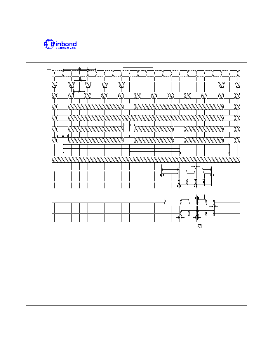
Figure26:READ WITHOUT AUTO PRECHARGE
READ-WITHOUT AUTO PRECHARGE
t
CK
t
CH
t
CL
CK
CK
CKE
NOP
NOP
t
IS
t
IH
COMMAND
t
IS
t
IH
t
IS
t
IH
A9,A10
Bank x
t
IS
t
IH
BA0,BA1
t
IS
t
IH
DIS AP
Col n
READ
DM
CL = 3
t
RP
DQS
DQ
DQS
DQ
max
DON'T CARE
t
RPST
t
DQSCK
min
t
RPRE
t
LZ
min
t
LZ
min
t
AC
DO
n
t
HZ
min
min
t
RPRE
t
LZ
max
DO
n
t
DQSCK
max
t
AC
t
RPST
t
HZ
max
ALL BANKS
ONE BANK
*Bank x
RA
Bank x
RA
RA
NOP
PRE
NOP
NOP
NOP
NOP
ACT
A8
A0-A7
t
AC
/t
DQSCK=max
t
AC
/t
DQSCK=min
DO n = Data Out from column n
Burst Length = 4
DIS AP = Disable Autoprecharge
* = "Don't Care", if A8 is HIGH at this point
PRE = PRECHARGE, ACT = ACTIVE, RA = Row Address, BA = Bank Address
NOP commands are shown for ease of illustration; other commands may be valid at these times
W946432AD
34
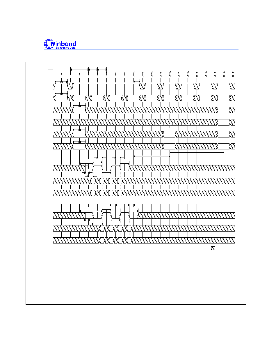
Figure27:READ - WITH AUTO PRECHARGE
READ-WITH AUTO PRECHARGE
t
CK
t
CH
t
CL
CK
CK
CKE
NOP
t
IS
t
IH
COMMAND
NOP
t
IS
t
IH
t
IS
t
IH
A9,A10
Bank x
t
IS
t
IH
BA0,BA1
EN AP
Col n
READ
DM
CL = 3
t
RP
NOP
DQS
DQ
DQS
DQ
DON'T CARE
A0-A7
A8
t
RPST
t
DQSCK
min
t
RPRE
t
LZ
min
t
LZ
min
t
AC
DO
n
t
HZ
min
min
max
t
RPRE
t
LZ
max
DO
n
t
DQSCK
max
t
AC
t
RPST
t
HZ
max
RA
RA
NOP
NOP
NOP
NOP
NOP
ACT
RA
Bank x
t
AC
/t
DQSCK=min
t
AC
/t
DQSCK=max
DO n = Data Out from column n
Burst Length = 4
EN AP = Enable Autoprecharge
ACT = ACTIVE, RA = Row Address
NOP commands are shown for ease of illustration; other commands may be valid at these times
W946432AD
35
Figure28:BANK READ ACCESS
BANK READ ACCESS
CK
CK
CKE
t
IS
t
IH
t
CK
t
CH
t
CL
NOP
ACT
READ
NOP
NOP
PRE
NOP
NOP
NOP
COMMAND
t
IS
t
IH
NOP
RA
Col n
RA
RA
RA
ALL BANKS
ONE BANK
Bank x
t
IS
t
IH
BA0,BA1
Bank x
*Bank x
DQS
DQ
t
RPST
t
DQSCK
min
t
RPRE
t
LZ
min
t
LZ
min
t
AC
DO
n
t
HZ
min
min
DQS
DQ
DON'T CARE
max
t
RPRE
t
LZ
max
DO
n
t
DQSCK
max
t
AC
t
RPST
t
HZ
max
DIS AP
t
IS
t
IH
t
RC
CL=3
t
RAS
t
RCD
t
RP
DM
A8
A9,A10
A0-A7
ACT
RA
RA
Bank x
t
AC
/t
DQSCK=min
t
AC
/t
DQSCK=max
DO n = Data Out from column n
Burst Length = 4
DIS AP = Disable Autoprecharge
* = "Don't Care", if A8 is HIGH at this point
PRE = PRECHARGE, ACT = ACTIVE, RA = Row Address, BA = Bank Address
NOP commands are shown for ease of illustration; other commands may be valid at these times
Note that tRCD MIN so that the same timing applies if Autoprecharge is enabled (in which case tRAS would be limiting)
W946432AD
36
Figure29:WRITE WITHOUT AUTO PRECHARGE
t
CK
t
CH
t
CL
CK
CK
CKE
NOP
NOP
t
IS
t
IH
COMMAND
t
IS
t
IH
t
IS
t
IH
A9,A10
Bank x
t
IS
t
IH
BA0,BA1
t
IS
t
IH
DIS AP
Col n
WRITE
ALL BANKS
ONE BANK
*Bank x
RA
BA
RA
RA
NOP
PRE
NOP
NOP
NOP
NOP
ACT
A8
A0-A7
t
IH
t
DQSS
t
DQSH
t
DSH
t
DSH
t
WPST
t
WR
t
RP
t
WPRES
t
WPRE
t
DQSL
t
DQSS
t
DQSH
t
DSS
t
DSS
t
WPST
t
WPRES
t
WPRE
t
DQSL
DQS
DQ
DM
DQS
DQ
DM
WRITE - WITHOUT AUTO PRECHARGE
DON'T CARE
DI
n
DI
n
t
DQSS=min
t
DQSS=max
DI n = Data IN from column n
Burst Length = 4
DIS AP = Disable Autoprecharge
* = "Don't Care", if A8 is HIGH at this point
PRE = PRECHARGE, ACT = ACTIVE, RA = Row Address, BA = Bank Address
NOP commands are shown for ease of illustration; other commands may be valid at these times

W946432AD
37
Figure30:WRITE WITH AUTO PRECHARGE
t
CK
t
CH
t
CL
CK
CK
CKE
NOP
NOP
t
IS
t
IH
COMMAND
t
IS
t
IH
t
IS
t
IH
A9,A10
Bank x
t
IS
t
IH
BA0,BA1
Col n
WRITE
RA
BA
RA
RA
NOP
NOP
NOP
NOP
NOP
ACT
A8
A0-A7
t
DQSS
t
DQSH
t
DSH
t
DSH
t
WPST
t
DAL
t
WPRES
t
WPRE
t
DQSL
t
DQSS
t
DQSH
t
DSS
t
DSS
t
WPST
t
WPRES
t
WPRE
t
DQSL
DQS
DQ
DM
DQS
DQ
DM
WRITE - WITH AUTO PRECHARGE
DON'T CARE
DI
n
DI
n
NOP
EN AP
t
DQSS=min
t
DQSS=max
DI n = Data IN from column n
Burst Length = 4
EN AP = Disable Autoprecharge
ACT = ACTIVE, RA = Row Address, BA = Bank Address
NOP commands are shown for ease of illustration; other commands may be valid at these times
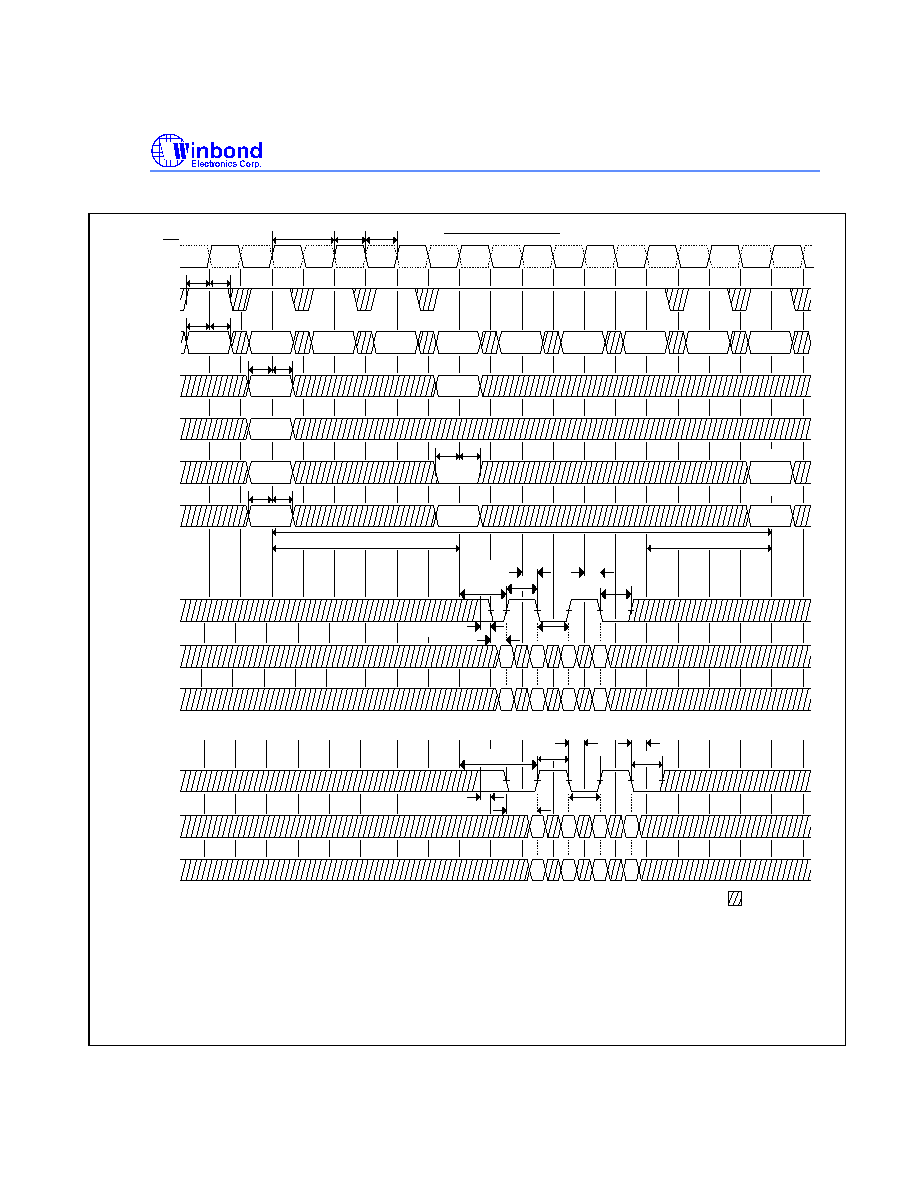
W946432AD
38
Figure31:BANK WRITE ACCESS
CK
CK
CKE
NOP
NOP
t
IS
t
IH
COMMAND
t
IS
t
IH
t
IS
t
IH
A9,A10
Bank x
t
IS
t
IH
BA0,BA1
Col n
WRITE
*Bank x
RA
NOP
PRE
NOP
NOP
NOP
NOP
ACT
A8
A0-A7
t
WR
t
RAS
BANK WRITE ACCESS
t
CK
t
CH
t
CL
RA
RA
ALL BANKS
ONE BANK
t
IS
t
IH
DIS AP
*Bank x
DQS
DQ
DM
DQS
DQ
DM
DON'T CARE
t
RCD
t
WPST
t
DSH
t
DSH
t
DQSS
t
DQSH
t
WPRES
t
WPRE
t
DQSL
DI
n
t
DQSS
t
DQSH
t
DSS
t
DSS
t
WPST
t
WPRES
t
WPRE
t
DQSL
DI
n
t
DQSS=min
t
DQSS=max
DI n = Data IN from column n
Burst Length = 4
DIS AP = Disable Autoprecharge
* = "Don't Care", if A8 is HIGH at this point
PRE = PRECHARGE, ACT = ACTIVE, RA = Row Address, BA = Bank Address
NOP commands are shown for ease of illustration; other commands may be valid at these times
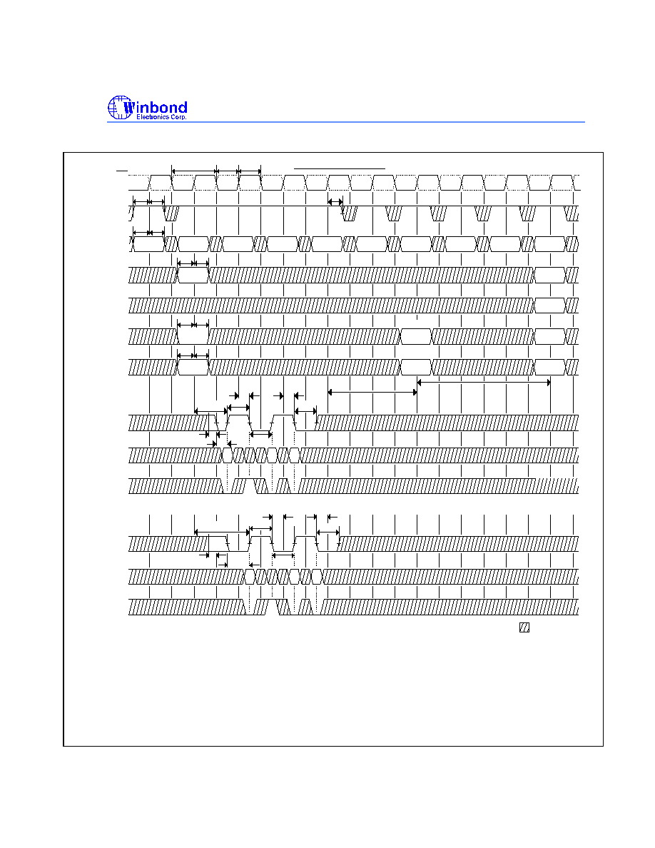
W946432AD
39
Figure32:WRITE DM OPERATION
t
CK
t
CH
t
CL
CK
CK
CKE
NOP
NOP
t
IS
t
IH
COMMAND
t
IS
t
IH
t
IS
t
IH
A9,A10
Bank x
t
IS
t
IH
BA0,BA1
t
IS
t
IH
DIS AP
Col n
WRITE
ALL BANKS
ONE BANK
*Bank x
RA
BA
RA
RA
NOP
PRE
NOP
NOP
NOP
NOP
ACT
A8
A0-A7
t
IH
t
DQSS
t
DQSH
t
DSH
t
DSH
t
WPST
t
WR
t
RP
t
WPRES
t
WPRE
t
DQSL
t
DQSS
t
DQSH
t
DSS
t
DSS
t
WPST
t
WPRES
t
WPRE
t
DQSL
DQS
DQ
DM
DQS
DQ
DM
WRITE - DM OPERATION
DON'T CARE
DI
n
DI
n
t
DQSS=min
t
DQSS=max
DI n = Data IN from column n
Burst Length = 4
DIS AP = Disable Autoprecharge
* = "Don't Care", if A8 is HIGH at this point
PRE = PRECHARGE, ACT = ACTIVE, RA = Row Address, BA = Bank Address
NOP commands are shown for ease of illustration; other commands may be valid at these times
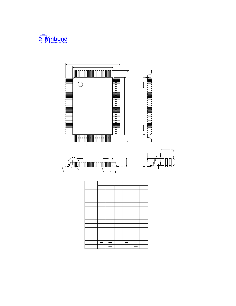
W946432AD
40
PACKAGE DIMENSIONS
E
H
y
A
A2
Seating Plane
L
L
1
See Detail F
Controlling dimension : Millimeters
A1
E
D
H
D
e
b
c
0.08
0
7
0
0.003
1.00
0.75
16.10
0.60
16.00
0.45
15.90
0.039
0.030
0.870
0.634
0.024
0.866
0.630
0.018
0.862
0.626
0.65
20.10
14.10
0.20
0.38
1.45
20.00
14.00
1.40
19.90
13.90
0.10
0.22
1.35
0.791
0.555
0.008
0.015
0.057
0.787
0.551
0.055
0.026
0.783
0.547
0.004
0.009
0.053
Symbol
Min Nom Max
Max
Nom
Min
Dimension in inch
Dimension in mm
A
b
c
D
e
H
D
H
E
L
y
A
A
L
1
1
2
E
0.013
0.006
0.15
0.32
21.90
22.00
22.10
7
0.020
0.032
0.498
0.802
0.10
0.05
0.002 0.004
0.006
0.15