
PRELIMINARY W925E/C625
8-bit CID Microcontroller
-1-
Release Date : 2002/5/13
Revision : A5
1
GENERAL DESCRIPTION...................................................................................................................... 3
2
FEATURES .................................................................................................................................................. 3
3
PIN CONFIGURATION............................................................................................................................ 5
4
PIN DESCRIPTION ................................................................................................................................... 6
5
BLOCK DIAGRAM ................................................................................................................................... 8
6
FUNCTIONAL DESCRIPTION .............................................................................................................. 9
6.1
M
EMORY
O
RGANIZATION
................................................................................................................... 10
6.2
S
PECIAL
F
UNCTION
R
EGISTERS
........................................................................................................... 13
6.3
I
NSTRUCTION
....................................................................................................................................... 30
6.4
P
OWER
M
ANAGEMENT
........................................................................................................................34
6.5
R
ESET
................................................................................................................................................... 35
6.6
I
NTERRUPT
........................................................................................................................................... 35
6.7
P
ROGRAMMABLE
T
IMERS
/C
OUNTERS
................................................................................................ 37
6.8
S
ERIAL
P
ORT
1 .....................................................................................................................................42
6.9
C
OMPARATOR
...................................................................................................................................... 43
6.10
DTMF G
ENERATOR
............................................................................................................................. 43
6.11
FSK G
ENERATOR
................................................................................................................................ 44
6.12
I/O P
ORTS
.............................................................................................................................................46
6.13
D
IVIDER
................................................................................................................................................46
6.14
LCD...................................................................................................................................................... 46
6.15
C
ALLING
I
DENTITY
D
ELIVERY
(CID) ................................................................................................. 50
7
ELECTRICAL CHARACTERISTICS .................................................................................................63
7.1
M
AXIMUM
R
ATINGS
* .......................................................................................................................... 63
7.2
R
ECOMMENDED
O
PERATING
C
ONDITIONS
......................................................................................... 63
7.3
DC E
LECTRICAL
C
HARACTERISTICS
.................................................................................................. 63
E
LECTRICAL
C
HARACTERISTICS
- G
AIN
C
ONTROL
OP-A
MPLIFIER
...............................................................65
7.4
AC E
LECTRICAL
C
HARACTERISTICS
.................................................................................................. 65
8
PACKAGE..................................................................................................................................................68

PRELIMINARY W925E/C625
8-bit CID Microcontroller
-2-
Release Date : 2002/5/13
Revision : A5
F
IGURE
3-1 W925E/C625 P
IN
C
ONFIGURATION
.................................................................................................. 5
F
IGURE
6-1 P
ROGRAM
M
EMORY
M
AP
................................................................................................................10
F
IGURE
6-2 M
EMORY
M
AP
.................................................................................................................................. 11
F
IGURE
6-3 S
CRATCHPAD
RAM/R
EGISTER
A
DDRESSING
.................................................................................. 12
F
IGURE
6-4 T
HE
S
TRUCTURE OF
CID F
LAGS
...................................................................................................... 36
F
IGURE
6-5 M
ODE
0 & M
ODE
1
OF
T
IMER
/C
OUNTER
0 & 1.............................................................................. 38
F
IGURE
6-6 M
ODE
2
OF
T
IMER
/C
OUNTER
0 & 1 ................................................................................................ 39
F
IGURE
6-7 W
ATCHDOG
T
IMER
...........................................................................................................................40
F
IGURE
6-8 T
IMING OF THE
S
ERIAL
P
ORT
1 I
NPUT
F
UNCTION
........................................................................... 42
F
IGURE
6-9 T
IMING OF THE
S
ERIAL
P
ORT
1 O
UTPUT
F
UNCTION
....................................................................... 43
F
IGURE
6-10 T
HE
C
ONFIGURATION OF
C
OMPARATOR
....................................................................................... 43
F
IGURE
6-11 T
HE
R
ELATION
B
ETWEEN
DTMF
AND
K
EYPAD
........................................................................... 44
F
IGURE
6-12 FSK M
ODULATOR
.......................................................................................................................... 45
F
IGURE
6-13 13/14-
BIT
D
IVIDER
......................................................................................................................... 46
F
IGURE
6-14 LCD
ALTERNATING FREQUENCY
(FLCD)
CIRCUIT DIAGRAM
...................................................... 47
F
IGURE
6-15
1/5 B
IAS
LCD P
OWER
C
ONNECTION
............................................................................................. 49
F
IGURE
6-16 LCD
WAVEFORM FOR
1/5
BIAS
...................................................................................................... 49
F
IGURE
6-17 T
HE
CID B
LOCK
D
IAGRAM
........................................................................................................... 50
F
IGURE
6-18 A
PPLICATION
C
IRCUIT OF THE
R
ING
D
ETECTOR
........................................................................... 51
F
IGURE
6-19 D
IFFERENTIAL
I
NPUT
G
AIN
C
ONTROL
C
IRCUIT
............................................................................52
F
IGURE
6-20 S
INGLE
-E
NDED
I
NPUT
G
AIN
C
ONTROL
C
IRCUIT
........................................................................... 52
F
IGURE
6-21 G
UARD
T
IME
W
AVEFORM OF
A
LERT
T
ONE
S
IGNAL
D
ETECTION
................................................53
F
IGURE
6-22 T
HE
W
AVEFORM OF
DTMF D
ETECTION
....................................................................................... 54
F
IGURE
6-23 FSK D
ETECTION
E
NABLE AND
FSK C
ARRIER
P
RESENT AND
A
BSENT
T
IMING
.......................... 54
F
IGURE
6-24 S
ERIAL
D
ATA
I
NTERFACE
T
IMING OF
FSK D
EMODULATION
....................................................... 55
F
IGURE
6-25 I
NTERNAL
CID G
AIN
C
ONTROL
R
EGISTER
S
ETTING
W
AVEFORM
............................................... 56
F
IGURE
6-26 A
PPLICATION
C
IRCUIT OF
CID ...................................................................................................... 57
F
IGURE
6-27 I
NPUT AND
O
UTPUT
T
IMING OF
B
ELLCORE
O
N
-
HOOK
D
ATA
T
RANSMISSION
............................. 58
F
IGURE
6-28 I
NPUT AND
O
UTPUT
T
IMING OF
B
ELLCORE
O
FF
-
HOOK
D
ATA
T
RANSMISSION
............................59
F
IGURE
6-29 I
NPUT AND
O
UTPUT
T
IMING OF
BT I
DLE
S
TATE
(O
N
-
HOOK
) D
ATA
T
RANSMISSION
.................. 60
F
IGURE
6-30 I
NPUT AND
O
UTPUT
T
IMING OF
BT L
OOP
S
TATE
(O
FF
-
HOOK
) D
ATA
T
RANSMISSION
............... 61
F
IGURE
6-31 I
NPUT AND
O
UTPUT
T
IMING OF
CCA C
ALLER
D
ISPLAY
S
ERVICE
D
ATA
T
RANSMISSION
.......... 62

PRELIMINARY W925E/C625
8-bit CID Microcontroller
-3-
Release Date : 2002/5/13
Revision : A5
1 GENERAL DESCRIPTION
The W925E/C625 is an all-in-1
single 8-bit micro-controller with
widely used Calling Identity
Delivery (CID) function. The 8-bit CPU core is based on the 8051 family; therefore, all the
instructions are compatible to the Turbo 8051 series. The CID part consists FSK decoder, DTMF
receiver,
CPE
*
Alert Signal (CAS
) detector and Ring detector. Also built-in
DTMF
generator
and
FSK generator with baud rate 1200 bps (bits/sec). Using W925E/C625 can easily implement the
CID adjunct box and the feature phone or
Short Message Service (SMS)
phone with CID
function. The main features are listed in the next section.
2 FEATURES
�
APPLICATION: The SMS phone with CID function and CID adjunct box.
�
CPU: 8-bit micro-controller is similar to the 8051 family.
- Operating voltage:
�
C: 2.2 to 5.5 volt.
CID: 3.0 to 5.5 volt.
�
Dual-clock operation:
- Main oscillator: 3.58MHz crystal for CID and DTMF function. And built-in RC oscillator.
- Sub oscillator: 32768Hz crystal.
- Main and sub oscillators are enable/disable by bit control individually.
�
ROM: 64K bytes internal flash EEPROM/MASK ROM type.
- up 64K bytes for program ROM.
- total 64K bytes for look-up table ROM.
�
RAM:
- 256 bytes on chip scratch-pad RAM.
- 4K bytes on chip RAM for MOVX instruction.
- 224 bytes on chip LCD RAM.
�
LCD: dot matrix control method.
- 1792 dots: 56 Segments x 32 Common, 1/5 bias.
�
CID:
- Compatible with Bellcore TR-NWT-000030 & SR-TSV-002476, British Telecom(BT)
SIN227, U.K. Cable Communication Association(CCA) specification.
-
FSK modulator/demodulator: for Bell 202 and ITU-T V.23
FSK with 1200 baud rate.
- CAS detector: for dual tones of Bellcore CAS and BT Idle State and Loop State Dual
Tone Alert Signal (DTAS).
- DTMF generator/receiver;
DTMF receiver can be programmed as a tone detector.
- Ring detector: for line reversal for BT, ring burst for CCA or ring signal for Bellcore.
- Two independent OP amps with adjustable gain for Tip/Ring and Telephone Hybrid
connections.
�
I/O: 40 I/O pins.
- P0: Bit and byte addressable. I/O mode can be bit controlled. Open drain type.
- P1~P3: Bit and byte addressable. Pull high and I/O mode can be bit controlled.
- P4 : Byte addressable . Pull high and I/O mode can be bit controlled.
note: "CPE*" Customer Premises Equipment

PRELIMINARY W925E/C625
8-bit CID Microcontroller
-4-
Release Date : 2002/5/13
Revision : A5
�
Power mode:
- Normal mode: Normal operation
- Dual-clock slow operation mode: System is operated by the sub-oscillator (Fosc=Fs
and Fm is stopped)
- Idle mode: CPU hold. The clock to the CPU is halted, but the interrupt, timer and
watchdog timer block work normally but CID function is disabled.
- Power down mode: All activity is completely stopped and power consumption is
less
than 1
�
A.
�
Timer: 2 13/16-bit timers, or 8-bit auto-reload timers, that are Timer0 and Timer1.
�
Watchdog timer:
WDT can be programmed by the user to serve as a system monitor
.
�
Interrupt: 11 interrupt sources with two levels of priority.
-
4 interrupts from INT0, INT1, INT2 and INT3.
- 2 interrupts from Timer0, Timer1.
- 1 interrupt from Serial port.
- 1 interrupt from CID.
- 1 interrupt from 13/14-bit Divider.
- 1 interrupt from Comparator.
- 1 interrupt from Watch Dog Timer.
�
Divider: 13/14 bit divider, clock source from sub-oscillator, therefore, DIVF set every 0.25/0.5
Sec.
�
Comparator:
- Comparator: 1 analog inputs from VNEG pin, 2 reference input pins, one is from VPOS
pin and another is from internal 1.0v regulator output.
�
Serial port:
- An 8-bit serial transceiver with SCLK and SDATA.
.
�
Package:
- 160pin QFP
PRELIMINARY W925E/C625
8-bit CID Microcontroller
-5-
Release Date : 2002/5/13
Revision : A5
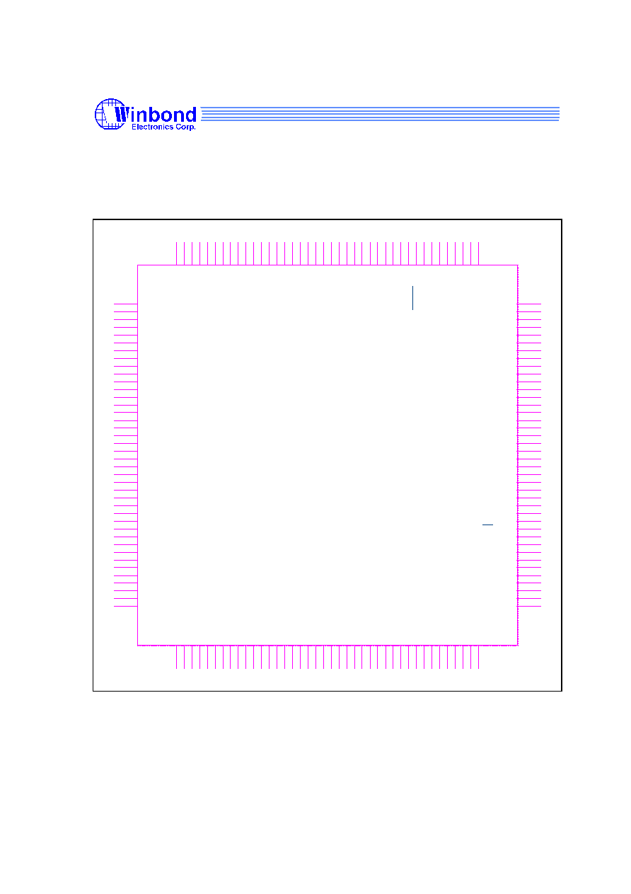
3 PIN CONFIGURATION
Figure 3-1 shows the pin assignment. The package type is 160pin QFP.
VSS
109
VDD
110
RNGDI
75
CAP
74
VREF
73
INP1
72
INN1
71
GCFB1
70
VAD
65
VAS
69
GCFB2
68
INN2
67
INP2
66
VSS
77
TEST/MODE
128
RESET/VPP
129
P10
93
P11
94
P12
95
P13
96
P14
97
P15
98
P16
99
P17
100
P20
101
P21
102
P22
103
P23
104
P24
105
P25
106
P26
107
P27
108
BUZ
111
P30
112
P31
113
P32
114
P33
115
P34
116
P35
117
P36
118
P37
119
P40
120
RNGRC
76
P07
85
P06
84
P05
83
P04
82
P03
81
P02
80
P01
79
P00
78
XOUT1
86
XIN1
87
VDD
88
XIN2
89
XOUT2
90
EA/DATA
91
DTMF/FSK
92
COM31
64
COM30
63
COM29
62
COM28
61
COM27
60
COM26
59
COM25
58
COM24
57
COM23
56
COM22
55
COM21
54
COM20
53
COM19
52
COM18
51
COM17
50
COM16
49
SEG55
48
SEG54
47
SEG53
46
SEG52
45
SEG51
44
SEG50
43
SEG49
42
SEG48
41
SEG47
40
SEG46
39
SEG45
38
SEG44
37
SEG43
36
SEG42
35
SEG41
34
SEG40
33
SEG39
32
SEG38
31
SEG37
30
SEG36
29
SEG35
28
SEG34
27
SEG33
26
SEG32
25
SEG31
24
SEG30
23
SEG29
22
SEG28
21
SEG27
20
SEG26
19
SEG25
18
SEG24
17
SEG23
16
SEG22
15
SEG21
14
SEG20
13
SEG19
12
SEG18
11
SEG17
10
SEG16
9
SEG15
8
SEG14
7
SEG13
6
SEG12
5
SEG11
4
SEG10
3
SEG9
2
SEG8
1
P41
121
P42/VNEG
122
P43
123
P44/VPOS
124
P45
125
P46
126
P47
127
DH2
130
DH1
131
VLCD1
132
VLCD2
133
VLCD3
134
VLCD4
135
VLCD5
136
COM15
137
COM14
138
COM13
139
COM12
140
COM11
141
COM10
142
COM9
143
COM8
144
COM7
145
COM6
146
COM5
147
COM4
148
COM3
149
COM2
150
COM1
151
COM0
152
SEG0
153
SEG1
154
SEG2
155
SEG3
156
SEG4
157
SEG5
158
SEG6
159
SEG7
160
W925E/C625
U?
Figure 3-1 W925E/C625 Pin Configuration