
Preliminary W81181D/AD
USB HUB CONTROLLER
Publication Release Date: October 1999
- 1 - Revision A1
W81181D/AD
USB HUB Controller

Preliminary W81181D/AD
- 2 -
W81181D Data Sheet Revision History
Pages
Dates
Version Version
on Web
Main Contents
1
N.A.
10/01/98
0.50
N.A.
First published.
2
3/15/99
0.60
Add pin configuration and pin description
3
3/30/99
0.61
Modify pin configuration & pin description
4
5/4/99
0.62
Modify reference schematic
5
5/13/99
0.63
Modify pin 12 description
6
5/26/1999
0.64
Modify feature HUB spec Rev 1.1
7
7/09/1999
0.65
Add 48 MHz clock input pinout
8
7/12/1999
0.66
Modify 48 MHz (W81181AD) Schematic
9
10
Please note that all data and specifications are subject to change without notice. All the trade
marks of products and companies mentioned in this data sheet belong to their respective
owners.
LIFE SUPPORT APPLICATIONS
These products are not designed for use in life support appliances, devices, or systems where
malfunction of these products can reasonably be expected to result in personal injury.
Winbond customers using or selling these products for use in such applications do so at their
own risk and agree to fully indemnify Winbond for any damages resulting from such
improper use or sales.

Preliminary W81181D/AD
Publication Release Date: October 1999
- 3 - Revision A1
Table of Contents-
1. GENERAL DESCRIPTION....................................................................................................................... 4
2. FEATURES................................................................................................................................................ 4
3. USB BLOCK DIAGRAM .......................................................................................................................... 5
4. PIN CONFIGURATION............................................................................................................................. 6
W81181D (12 MH
Z
C
LOCK
I
NPUT
) ............................................................................................................. 6
W81181AD (48 MH
Z
C
LOCK
I
NPUT
)........................................................................................................... 7
5. PIN DESCRIPTION................................................................................................................................... 8
W81181D:................................................................................................................................................... 8
W81181AD: .............................................................................................................................................. 10
IO TYPE: ..................................................................................................................................................12
6. ABSOLUTE MAXIMUM RATINGS........................................................................................................12
7. ELECTRICAL CHARACTERISTICS.....................................................................................................13
8. TYPICAL APPLICATION .......................................................................................................................15
W81181D:................................................................................................................................................. 15
W81181AD: .............................................................................................................................................. 16
10. PACKAGE DIMENSIONS....................................................................................................................18
Preliminary W81181D/AD
- 4 -
1. GENERAL DESCRIPTION
W81181D, an high integrated 4 port USB hub controller which integrates a microcontroller,
implements a medium speed (12 MHz) and slow speed (1.5 MHz) Universal Serial Bus (USB) hub
control interface. It supports one upstream, four downstream ports and a serial interface. W81181D
can be act as multifunction USB device. For example, the whole system can be designed as an USB
HUB plus an USB mouse or an USB HUB plus an IR receiver, and no down stream port be occupied
as well as no other component needed.
W81181D acts as an USB hub controller and a hub repeater at the direction of an internal
microcontroller. W81181D controls the traffic among the host, four downstream ports, and the
microprocessor. As a hub controller, it can enable/disable ports, send and receive resets, and detect
devices of high or low speeds. The W81181D contains three function endpoints and two hub
endpoints to allow both USB Control and Interrupt Transfers between the host and microcontroller.
W81181D is a compound USB device (hub with embedded function attached) with totally five
downstream ports. W81181D can be used as a hub controller in a standalone hub with attached
function or a microcontroller based USB device with hub function.
Ordering Information
PART NO.
INPUT CLOCK Freq.
PACKAGE
W81181D
12 MHz
48-LQFP
W81181AD
48 MHz
48-LQFP
2. FEATURES
�
Full compliance with USB spec Rev 1.1 and HID Class Definition Rev 1.0
�
Compliance with USB Hub spec Rev 1.1
�
Support multiple endpoints for standalone hub with attached function
�
Embedded microprocessor--8052 ( 6K ROM + 256 Byte RAM)
�
Support auto-detected two power source mode between bus power mode and self power mode.
�
12-MHz crystal/oscillator input to lower EMI (W81181D)
�
48-Mhz oscillator input for motherboard application (W81181AD)
�
Support Suspend and Resume operation
�
Four downstream ports with per port overcurrent protection
�
Two endpoints for hub (Control and Interrupt)
�
LED display supports bright/blinking alternative for port enable and OCP(over current protection)
flags
�
Single 5V supplied with embedded 5V-3.3V regulator
�
Three endpoints for attached device (one Control and two Interrupt)
�
Provides the external pull-up resistor control for the up-stream connection.
�
Perport/Global downstream port power control optional
�
Packaged in 48-pin LQFP
�
5V CMOS device

Preliminary W81181D/AD
Publication Release Date: October 1999
- 5 - Revision A1
3. USB BLOCK DIAGRAM
The Serial Interface Engine (SIE) controls the USB data flow between the uCs and the USB bus. Port0
is a high speed (HS) transceiver for the upstream data path. The Hub Repeater is the traffic controller
which directs the bus data to and from the correct paths. The hub Controller and Function Controller
determines what data is to be written to or read from the various FIFOs. The Bus Controller directs the
interface between the uC and Hub/Function Controller.
UPSTREAM PORT
TRANCEIVER
PORT 0
SERIAL
INTERFACE
ENGINE
FUNCTION
CONTROLLER
HUB
CONTROLLER
HUB
REPEATER
TRANCEIVER
PORT 1
TRANCEIVER
PORT 2
TRANCEIVER
PORT 3
TRANCEIVER
PORT 4
USB FIFOs
BUS
CONTROLLER
DOWNSTREAM DEVICES
uC
Preliminary W81181D/AD
- 6 -
4. PIN CONFIGURATION
W81181D (12 MHz Clock Input)
1
12
13
24
25
36
37
48
VDD3V
VDDA
GNDA
VBUS
LEDOC4_
LEDOC3_
LEDOC2_
LEDOC1_
VDD
RESET
P3[3]/INT1_
P1[0]/SACK/INDIV
P1[1]/SSTB
LEDEN5_
LEDEN4_
OCP4_
EXTPUEN
VDD
XTAL2
XTAL1
GND
LEDEN1_
LEDEN2_
LEDEN3_
PWEN4_
OCP3_
PWEN3_
LEDEN0_
OCP2_
PWEN2_
GND
OCP1_
PWEN1_
FWKP5
P1[2]/FSUSP5/BUSPWR
GND3V
DP4
DM4
DP3
DM3
GND3V
DP2
DM2
DP1
DM1
DP0
DM0
GND3V
W81181D
Preliminary W81181D/AD
Publication Release Date: October 1999
- 7 - Revision A1
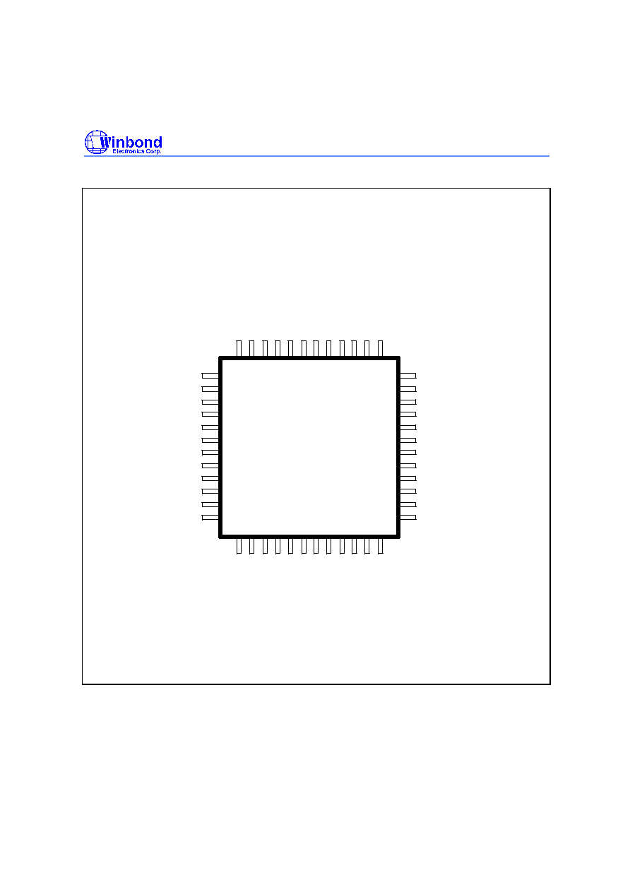
W81181AD (48 MHz Clock Input)
1
12
13
24
25
36
37
48
VDD3V
VDDA
GNDA
VBUS
LEDOC4_
LEDOC3_
LEDOC2_
LEDOC1_
VDD
RESET
P3[3]/INT1_
P1[0]/SACK/INDIV
P1[1]/SSTB
LEDEN5_
LEDEN4_
OCP4_
EXTPUEN
VDD
48CLKIN
GND
LEDEN1_
48CLKEN_
LEDEN2_
LEDEN3_
PWEN4_
OCP3_
PWEN3_
LEDEN0_
OCP2_
PWEN2_
GND
OCP1_
PWEN1_
FWKP5
P1[2]/FSUSP5/BUSPWR
GND3V
DP4
DM4
DP3
DM3
GND3V
DP2
DM2
DP1
DM1
DP0
DM0
GND3V
W81181AD

Preliminary W81181D/AD
- 8 -
5. PIN DESCRIPTION
W81181D
PIN
NUMBER
PAD
NAME
I/O TYPE
PIN FUNCTION
PULL UP/
DOWN
1
VDD3V
Power1
3.3V Regulator output. Supply voltage for all
transceivers.
-
2
VDDA
Power1
Analog power.
-
3
GNDA
Power0
Analog ground.
-
4
VBUS
IUD2T
Input of upstream power status. On self-power mode,
connection should be controlled by VBUS status.
-
5
LEDOC4_
IOU2P
Flag of port4 over-current. To drive LED directly
O
6
LEDOC3_
IOU2P
Flag of port3 over-current. To drive LED directly
O
7
LEDOC2_
IOU2P
Flag of port2 over-current. To drive LED directly
O
8
LEDOC1_
IOU2P
Flag of port1 over-current. To drive LED directly
O
9
VDD
Power1
Digital supply voltage.
-
10
RESET
IUD2T
Master reset input. Active high.
-
11
P3[3]/
INT1_
IOUD2
Normally, this pin is P33/INT1_ and used as bi-
directional serial data (SDATA) for embedded function
serial port.
U
12
P1[0]/
SACK/
INDIV
IOUD2
Normally, this pin is P10 and used as bi-directional
serial data ACK (SACK) for embedded function serial
port. If no embedded function this pin is INDIVIDUAL
(default) or GANGED mode setting for downstream
power control.
U
13
P1[1]/
SSTB
IOUD2
Normally, this pin is P11 and used as bi-directional
serial data Strobe (SSTB) for embedded function
serial port.
U
14
LEDEN5_
IOU2P
Downstream port5 LED. Active low to drive
bright/blinking LED when port5 enable.
O
15
LEDEN4_
IOU2P
Downstream port4 LED. Active low to drive
bright/blinking LED when port4 enable.
O
16
LEDEN3_
IOU2P
Downstream port3 LED. Active low to drive
bright/blinking LED when port3 enable.
O
17
LEDEN2_
IOU2P
Downstream port2 LED. Active low to drive
bright/blinking LED when port2 enable.
O
18
LEDEN1_
IOU2P
Downstream port1 LED. Active low to drive
bright/blinking LED when port1 enable.
O
19
GND
Power0
Digital ground
-
20
XTAL1
OSCM
Crystal IN. For 12 MHz oscillation.
-

Preliminary W81181D/AD
Publication Release Date: October 1999
- 9 - Revision A1
Pin Description ( W81181D ), continued
PIN
NUMBER
PAD NAME
I/O
TYPE
PIN FUNCTION
PULL UP/
DOWN
21
XTAL2
OSCM
Crystal OUT. For 12 MHz oscillation.
-
22
VDD
Power1 Digital supply voltage.
23
EXTPUEN
O2
External pull-up connection control.
O
24
OCP4_
IUD2T
Downstream port4 over-current status. Active low.
-
25
PWEN4_
O2
Downstream port4 power control. Active low.
O
26
OCP3_
IUD2T
Downstream port3 over-current status. Active low.
-
27
PWEN3_
O2
Downstream port3 power control. Active low.
O
28
LEDEN0_
IOU2P
Upstream port0 LED. Active low to drive
bright/blinking LED when upstream port0 enable.
O
29
OCP2_
IUD2T
Downstream port2 over-current status. Active low.
-
30
PWEN2_
O2
Downstream port2 power control. Active low.
O
31
GND
Power0 Digital ground.
32
OCP1_
IUD2T
Downstream port1 over-current LED. Active low.
-
33
PWEN1_
O2
Downstream port1 power control. Active low.
O
34
FWKP5
IUD2
Embedded function wake-up input.
D
35
P1[2]/
FSUSP5/
PWRDET
IOUD2
Normally, this pin is a P12 and used as embedded
function suspend control. If no embedded function
this pin is self-powered (High) or bus-powered
(Low) hub setting.
36
GND3V
Power0 Ground of port3 and port4 transceivers.
-
37
DP4
AIO
USB D+ for downstream port4.
-
38
DM4
AIO
USB D- for downstream port4.
-
39
DP3
AIO
USB D+ for downstream port3.
-
40
DM3
AIO
USB D- for downstream port3.
-
41
GND3V
Power0 Ground of port1 and port2 transceivers.
-
42
DP2
AIO
USB D+ for downstream port2.
-
43
DM2
AIO
USB D- for downstream port2.
-
44
DP1
AIO
USB D+ for downstream port1.
-
45
DM1
AIO
USB D- for downstream port1.
-
46
GND3V
Power0 Ground of port0 transceivers.
-
47
DP0
AIO
USB D+ for upstream port0.
-
48
DM0
AIO
USB D- for upstream port0.
-

Preliminary W81181D/AD
- 10 -
W81181AD
PIN
NUMBER
PAD NAME
I/O
TYPE
PIN FUNCTION
PULL UP/
DOWN
1
V
DD
3V
Power1 3.3V Regulator output. Supply voltage for all
transceivers.
-
2
V
DD
A
Power1 Analog power.
-
3
GNDA
Power0 Analog ground.
-
4
VBUS
IUD2T
Input of upstream power status. On self-power
mode, connection should be controlled by VBUS
status.
-
5
LEDOC4_
IOU2P
Flag of port4 over-current. To drive LED directly
O
6
LEDOC3_
IOU2P
Flag of port3 over-current. To drive LED directly
O
7
LEDOC2_
IOU2P
Flag of port2 over-current. To drive LED directly
O
8
LEDOC1_
IOU2P
Flag of port1 over-current. To drive LED directly
O
9
V
DD
Power1 Digital supply voltage.
-
10
RESET
IUD2T
Master reset input. Active high.
-
11
P3[3]/
INT1_
IOUD2
Normally, this pin is P33/INT1_ and used as bi-
directional serial data (SDATA) for embedded
function serial port.
U
12
P1[0]/
SACK/
INDIV
IOUD2
Normally, this pin is P10 and used as bi-directional
serial data ACK (SACK) for embedded function
serial port. If no embedded function this pin is
INDIVIDUAL (default) or GANGED mode setting for
downstream power control.
U
13
P1[1]/
SSTB
IOUD2
Normally, this pin is P11 and used as bi-directional
serial data Strobe (SSTB) for embedded function
serial port.
U
14
LEDEN5_
IOU2P
Downstream port5 LED. Active low to drive
bright/blinking LED when port5 enable.
O
15
LEDEN4_
IOU2P
Downstream port4 LED. Active low to drive
bright/blinking LED when port4 enable.
O
16
LEDEN3_
IOU2P
Downstream port3 LED. Active low to drive
bright/blinking LED when port3 enable.
O
17
LEDEN2_
IOU2P
Downstream port2 LED. Active low to drive
bright/blinking LED when port2 enable.
O
18
48CLKEN_
IUD2
High enable embedded DPLL (12 MHz to 48 MHz).
It should be kept to Low when using 48Mhz clock.
U
19
LEDEN1_
IOU2P
Downstream port1 LED. Active low to drive
bright/blinking LED when port1 enable.
O
20
GND
Power0 Digital ground
-

Preliminary W81181D/AD
Publication Release Date: October 1999
- 11 - Revision A1
Pin Description ( W81181AD ), continued
PIN
NUMBER
PAD NAME
I/O
TYPE
PIN FUNCTION
PULL UP/
DOWN
21
48CLKIN
OSCM
Clock input for 48 MHz oscillation.
-
22
V
DD
Power1 Digital supply voltage.
23
EXTPUEN
O2
External pull-up connection control.
O
24
OCP4_
IUD2T
Downstream port4 over-current status. Active low.
-
25
PWEN4_
O2
Downstream port4 power control. Active low.
O
26
OCP3_
IUD2T
Downstream port3 over-current status. Active low.
-
27
PWEN3_
O2
Downstream port3 power control. Active low.
O
28
LEDEN0_
IOU2P
Upstream port0 LED. Active low to drive
bright/blinking LED when upstream port0 enable.
O
29
OCP2_
IUD2T
Downstream port2 over-current status. Active low.
-
30
PWEN2_
O2
Downstream port2 power control. Active low.
O
31
GND
Power0 Digital ground.
32
OCP1_
IUD2T
Downstream port1 over-current LED. Active low.
-
33
PWEN1_
O2
Downstream port1 power control. Active low.
O
34
FWKP5
IUD2
Embedded function wake-up input.
D
35
P1[2]/
FSUSP5/
PWRDET
IOUD2
Normally, this pin is a P12 and used as embedded
function suspend control. If no embedded function
this pin is self-powered (High) or bus-powered
(Low) hub setting.
36
GND3V
Power0 Ground of port3 and port4 transceivers.
-
37
DP4
AIO
USB D+ for downstream port4.
-
38
DM4
AIO
USB D- for downstream port4.
-
39
DP3
AIO
USB D+ for downstream port3.
-
40
DM3
AIO
USB D- for downstream port3.
-
41
GND3V
Power0 Ground of port1 and port2 transceivers.
-
42
DP2
AIO
USB D+ for downstream port2.
-
43
DM2
AIO
USB D- for downstream port2.
-
44
DP1
AIO
USB D+ for downstream port1.
-
45
DM1
AIO
USB D- for downstream port1.
-
46
GND3V
Power0 Ground of port0 transceivers.
-
47
DP0
AIO
USB D+ for upstream port0.
-
48
DM0
AIO
USB D- for upstream port0.
-

Preliminary W81181D/AD
- 12 -
IO TYPE
IO TYPE
DESCRIPTION
Power1
Power
Power0
Ground
OSCM
Middle-freq. Oscillating IO
IUD2
Input with pull-up/pull-down control
IUD2T
Schmitt Input with pull-up/pull-down control
IOU2P
Bi-directional high driving IO with programmable pull-up control and serial resistor
IOUD2
Bi-directional IO with pull-up/pull-down control
O2
Output
AIO
Analog Transceiver IO
Pull Up/Down Control
NOTE
DESCRIPTION
O
Output pin without pull-up/down
D
Input pin or I/O pin with pull-down
U
Input pin or I/O pin with pull-up
-
Input pin or I/O pin without pull-up/down
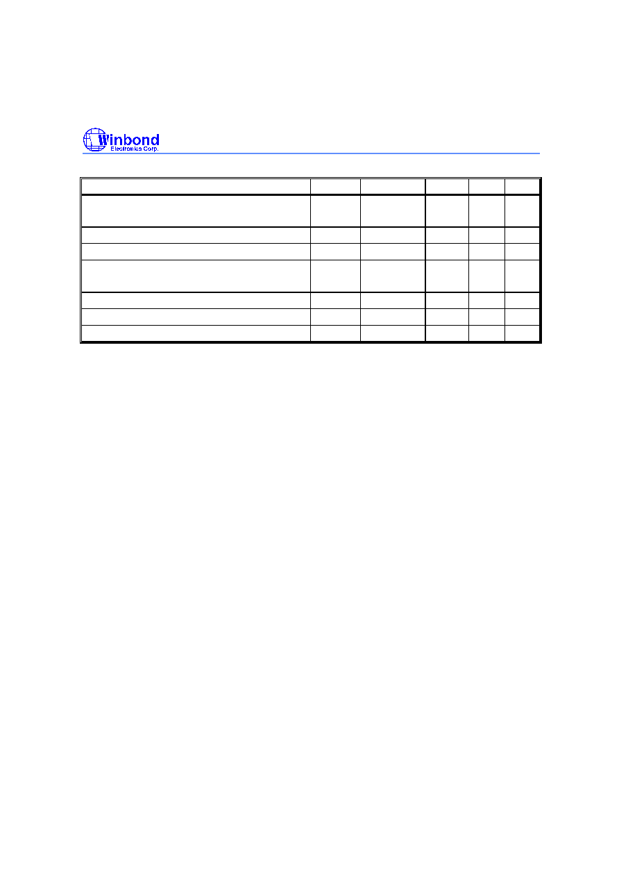
6. ABSOLUTE MAXIMUM RATINGS
PARAMETER
LIMIT
Supply Voltage (Vcc to Vss)
5.5V
Analog Input Voltage
Vss -0.5V to Vcc +0.5V
Digital Input Voltage
Vss -0.5V to Vcc +0.5V
Power Dissipation
TBD
Ambient Operating Temperature
0
o
C to 70
o
C
Lead Temperature (Soldering, 10 sec)
250
o
C
Note: Exposure to conditions beyond those listed under Absolute Maximum Ratings may adversely affect the life and reliability
of the device.

Preliminary W81181D/AD
Publication Release Date: October 1999
- 13 - Revision A1
7. ELECTRICAL CHARACTERISTICS
Operating Conditions
V
CC
= 5V +/-5%, T
A
= 0
o
to 70
o
C
PARAMETER
SYM.
CONDITIONS
MIN. MAX.
UNIT
V
CC
Supply Current
I
CC
TBD
mA
Logic Output High
V
OH
Io > 24 mA
2.5
V
CC
V
Logic Output Low
V
OL
Io > 6 mA
0.4
V
Logic Input Leakage Current
T
A
= 70
o
C
10
uA
USB CHARACTERISTICS
Note 8
Leakage Current:
Hi-Z State Output Leakage
I
LO
V< V
IN
< 3.3V
-10
+10
uA
Input Levels:
Differential Input Sensitivity
V
DI
|(D+)-(D-)|
0.2
V
Single Ended Signal "0"
V
SE0
0.8
2.0
V
Differential Common Mode Range
V
CM
Includes VDI range
0.8
2.5
Output Levels:
Driver Output Low
V
OLU
R
L
of 1.5 K
to 3.6V
0.3
V
Driver Output High
V
OHU
R
L
of 15 K
to GND
2.8
3.6
V
Output Signal Crossover Voltage
V
CRS
1.3
2.0
V
Capacitance:
Transceiver Capacitance
C
IN
Pin to GND
20
pF
Full Speed Timings:
Output Rise/Fall Times
t
R
/t
F
Notes 1, 4 (C
L
= 50 pF)
4
20
nS
Source Differential Driver Jitter to Next
Transition
/to Paired Transition
t
DJ1
/t
DJ2
Notes 2, 3
-3.5
/-4
3.5
/4
nS
nS
Differential to EOP transition Skew
t
DEOP
Note 3
-2
5
nS
Hub Differential Data Delay(without
cable)
t
HDD2
Notes 2, 3, 5
44
ns
Hub Differential Driver Jitter to Next
Transition
/to Paired Transition (including cable)
t
HDJ1
/t
HDJ2
Notes 2, 3, 5
-3
/-1
3
/1
nS
Data bit width distortion after SOP
t
SOP
Notes 3, 5
-5
5
nS
Hub SE0 Delay Relative to t
HDD
t
EOPD
Notes 3, 5
0
15
nS
Hub EOP Output Width Skew
t
HESK
Notes 3, 5
-15
15
nS
Low Speed Timings:
Output Rise/Fall Times
t
R
/t
F
Notes 1, 4 (C
L
= 50 pF)
75
300
nS
Preliminary W81181D/AD
- 14 -
Electrical Characteristics, continued
PARAMETER
SYM. CONDITIONS MIN.
MAX. UNIT
Source Differential Driver Jitter to Next Transition
/to Paired Transition
t
DJ1
/t
DJ2
Notes 2, 3
-25
/-14
25
/14
nS
nS
Differential to EOP transition Skew
t
DEOP
Notes 3
-40
100
nS
Hub Differential Data Delay(without cable)
t
HDD2
Notes 2, 3, 5
300
nS
Hub Differential Driver Jitter to Next Transition
/to Paired Transition (including cable)
t
HDJ1
/t
HDJ2
Notes 2, 3, 5
-45
/-45
45
/-45
nS
Data bit width distortion after SOP
t
SOP
Notes 3, 5
-60
60
nS
Hub SE0 Delay Relative to t
HDD
t
EOPD
Notes 3, 5
0
200
nS
Hub EOP Output Width Skew
t
HESK
Notes 3, 5
-300
300
nS
Notes:
1. Measured from 10% to 90% of the data signal.
2. Timing difference between the differential signals.
3. Measured at crossover point of differential data signals.
4. The rising and falling edges should be smoothly transiting(monotonic)
5. Full Speed timing have a 1.5 k
pull-up to 2.8 V on the D+ (DP) data line.
6. Low Speed timing have a 1.5 k
pull-up to 2.8 V on the D- (DM) data line.
7. The maximum load specification is the maximum effective capacitive load allowed that meets the target hub VBUS droop of
330 mV.
8. All other USB Electrical Characteristics refer to USB spec Rev 1.1 7.3.2 and 7.3.3.
Preliminary W81181D/AD
Publication Release Date: October 1999
- 15 - Revision A1
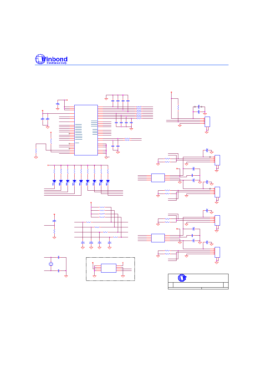
8. TYPICAL APPLICATION
W81181D
W81181D Reference Schematic
2.1
1
1
Friday, July 09, 1999
Size
Document Number
Rev
Date:
Sheet
of
VCC
VCC
VCC
VDD3
VBUS
VCC
VBUS
VCC
VCC2
VCC2
VCC
W81181D USB Hub Reference Schematic (Pure Hub)
Vendor ID / Product ID build in EEPROM
D-
D+
D1-
D1+
D2-
D1-
D1+
D-
D+
PW1
PW2
FL1
FL2
D2-
D2+
FL3
FL4
D3-
D3+
PWEN3
PW3
FL3
FL4
PWEN4
PW4
D4-
D4+
SCL
SDA
FL2
PWEN2
PWEN1
FL1
X2
D3-
OCP3
LEDEN3
OCP4
LEDOC1
LEDEN2
RESET
LEDOC2
X1
OCP1
SCL
LEDEN1
PWEN2
D2+
OCP4
PWEN3
LEDOC1
RESET
LEDEN1
PWRDET
D3+
EXTPUEN
LEDHUB
LEDOC2
LEDOC3
LEDEN4
D4-
PWEN4
X1
OCP1
OCP2
LEDOC4
LEDOC4
D4+
LEDEN2
SDA
LEDEN3
LEDOC3
LEDHUB
X2
OCP2
PWEN1
LEDEN4
OCP3
D1
LED
D2
LED
D3
LED
D4
LED
D5
LED
C1
120u
+
C2
120u
+
C3
0.1u
R1
15K
R2
15K
R3
15K
R4
15K
C4
120u
+
C5
120u
+
C6
0.1u
R5
15K
R6
15K
R7
15K
R8
15K
Y1
12MHz
WINBOND ELECTRONICS CORP.
inbond
C7
10u
+
C8
10u
+
R13
30
R14
30
R15
30
C9
15p
C10
15p
C11
15p
C12
15p
C13
15p
C14
15p
C15
15p
C16
15p
C17
15p
C18
15p
R21
30
R22
30
D6
LED
D7
LED
D8
LED
D9
LED
U1
24LC04B
A0
1
A1
2
A2
3
VSS
4
SDA
5
SCL
6
RC
7
VCC
8
C30
0.1u
+
C31
0.1u
+
C32
0.1u
+
C33
0.1u
+
USB3
USB(A)
1
2
3
4
5
6
C34
10u
+
C35
0.1u
+
C36
0.1u
+
R23
10K
R24
10K
R25
10K
R26
10K
R27
10K
R28
10K
R29
10K
R30
10K
C37
0.1u
+
C38
0.1u
+
C39
0.1u
+
C40
0.1u
+
R31
27K
C41
30p
C42
30p
R34
220
R35
220
R36
220
R37
220
R38
220
R39
220
R40
220
R41
220
R42
220
R43
3.3K
USB5
USB(A)
1
2
3
4
5
6
USB4
USB(A)
1
2
3
4
5
6
C29
0.1u
+
USB2
USB(A)
1
2
3
4
5
6
U2
AIC1526-0
C/A
1
F/A
2
F/B
3
C/B
4
O/A
8
IN
7
GND
6
O/B
5
U3
AIC1526-0
C/A
1
F/A
2
F/B
3
C/B
4
O/A
8
IN
7
GND
6
O/B
5
USB1
USB(B)
1
2
3
4
5
6
R33
7.5K
R17
30
R20
30
R18
30
R19
30
R16
30
R32
4.7K
U4
W81181D-48LQFP
VDD
9
XTAL1
20
LEDEN2
17
LEDEN3
16
LEDEN4
15
LEDEN5
14
LEDOC1
8
DM1
45
DP1
44
DM2
43
DP2
42
DM3
40
DP3
39
DM4
38
DP4
37
PWEN1
33
PWEN2
30
PWEN3
27
PWEN4
25
OCP2
29
OCP3
26
OCP4
24
LEDOC3
6
LEDOC4
5
SACK/INDIV
12
PWRDET/FSUS5
35
GNDA
3
GND3V
36
GND3V
41
LEDOC2
7
LEDEN0
28
SSTB/P11
13
LEDEN1
18
RESET
10
XTAL2
21
OCP1
32
INT1/P33
11
FWKP5
34
VDD
22
VDDA
2
VDD3V
1
GND3V
46
EXTPUEN
23
VBUS
4
DM0
48
DP0
47
GND
31
GND
19
Preliminary W81181D/AD
- 16 -
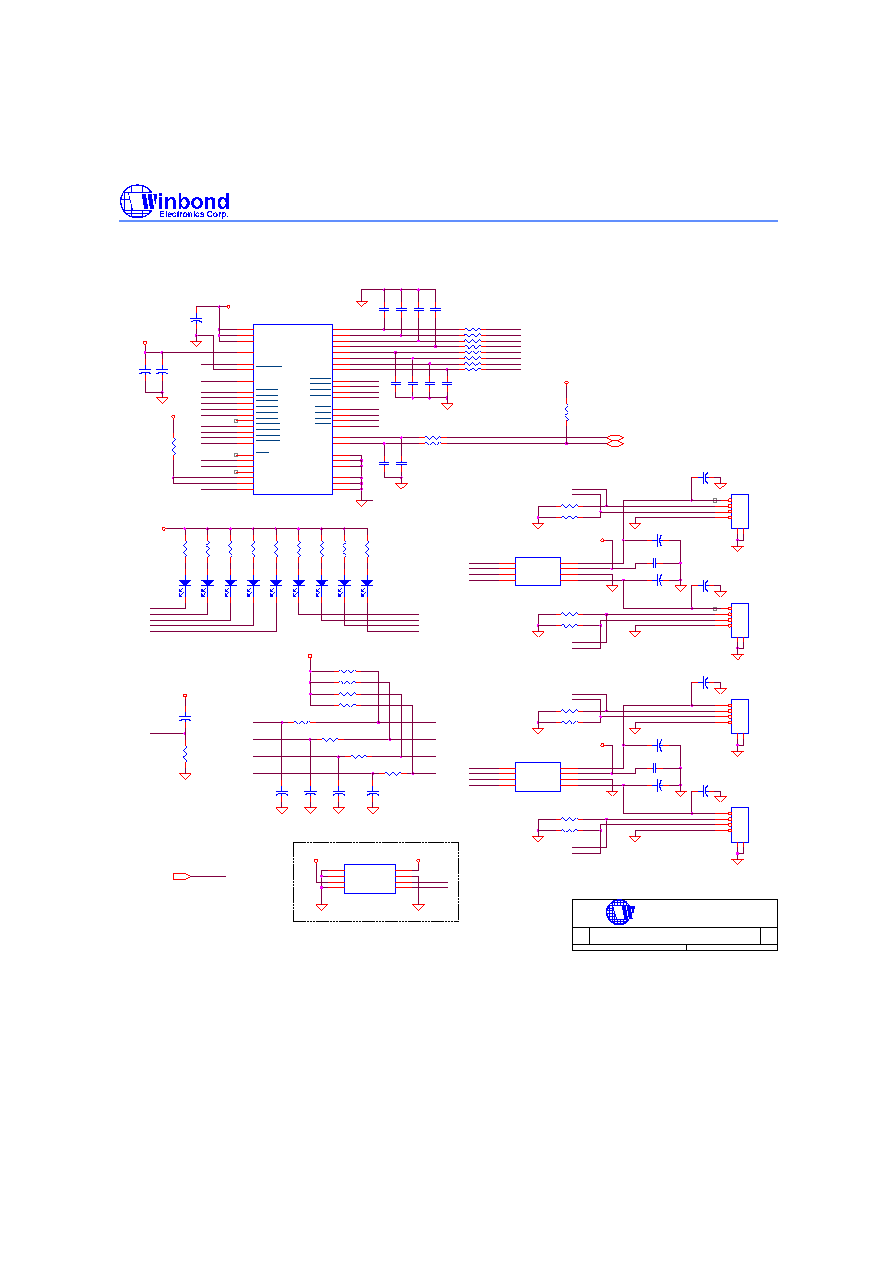
W81181AD
W81181AD Reference Schematic
2.2
1
1
Monday, July 12, 1999
Size
Document Number
Rev
Date:
Sheet
of
VCC
VCC
VCC
VDD3
VCC
VCC
VCC
VCC
VCC
VCC
VCC
Vendor ID / Product ID build in EEPROM
W81181AD USB Hub Reference Schematic (48MHz for Mother Board)
D1-
D1+
D2-
D1-
D1+
PW1
PW2
FL1
FL2
D2-
D2+
FL3
FL4
D3-
D3+
PWEN3
PW3
FL3
FL4
PWEN4
PW4
D4-
D4+
SCL
SDA
FL2
PWEN2
PWEN1
FL1
D3-
OCP3
LEDEN3
OCP4
LEDOC1
LEDEN2
RESET
LEDOC2
OCP1
SCL
LEDEN1
PWEN2
D2+
OCP4
PWEN3
LEDOC1
RESET
LEDEN1
D3+
EXTPUEN
LEDHUB
LEDOC2
LEDOC3
LEDEN4
D4-
PWEN4
X1
OCP1
OCP2
LEDOC4
LEDOC4
D4+
LEDEN2
SDA
LEDEN3
LEDOC3
LEDHUB
OCP2
PWEN1
LEDEN4
OCP3
X1
D1
LED
D2
LED
D3
LED
D4
LED
D5
LED
C1
120u
+
C2
120u
+
C3
0.1u
R1
15K
R2
15K
R3
15K
R4
15K
C4
120u
+
C5
120u
+
C6
0.1u
R5
15K
R6
15K
R7
15K
R8
15K
WINBOND ELECTRONICS CORP.
inbond
C7
10u
+
C8
10u
+
R13
30
R14
30
R15
30
C9
15p
C10
15p
C11
15p
C12
15p
C13
15p
C14
15p
C15
15p
C16
15p
C17
15p
C18
15p
R21
30
R22
30
D6
LED
D7
LED
D8
LED
D9
LED
U1
24LC04B
A0
1
A1
2
A2
3
VSS
4
SDA
5
SCL
6
RC
7
VCC
8
C30
0.1u
+
C31
0.1u
+
C32
0.1u
+
USB3
USB(A)
1
2
3
4
5
6
C35
0.1u
+
C36
0.1u
+
R23
10K
R24
10K
R25
10K
R26
10K
R27
10K
R28
10K
R29
10K
R30
10K
C37
0.1u
+
C38
0.1u
+
C39
0.1u
+
C40
0.1u
+
R34
220
R35
220
R36
220
R37
220
R38
220
R39
220
R40
220
R41
220
R42
220
R43
3.3K
USB5
USB(A)
1
2
3
4
5
6
USB4
USB(A)
1
2
3
4
5
6
C29
0.1u
+
USB2
USB(A)
1
2
3
4
5
6
U2
AIC1526-0
C/A
1
F/A
2
F/B
3
C/B
4
O/A
8
IN
7
GND
6
O/B
5
U3
AIC1526-0
C/A
1
F/A
2
F/B
3
C/B
4
O/A
8
IN
7
GND
6
O/B
5
R33
7.5K
R17
30
R20
30
R18
30
R19
30
R16
30
R32
4.7K
U4
W81181AD-48LQFP
VDD
9
48CLKIN
21
LEDEN2
17
LEDEN3
16
LEDEN4
15
LEDEN5
14
LEDOC1
8
DM1
45
DP1
44
DM2
43
DP2
42
DM3
40
DP3
39
DM4
38
DP4
37
PWEN1
33
PWEN2
30
PWEN3
27
PWEN4
25
OCP2
29
OCP3
26
OCP4
24
LEDOC3
6
LEDOC4
5
SACK/INDIV
12
PWRDET/FSUS5
35
GNDA
3
GND3V
36
GND3V
41
LEDOC2
7
LEDEN0
28
SSTB/P11
13
LEDEN1
19
RESET
10
48CLKEN
18
OCP1
32
INT1/P33
11
FWKP5
34
VDD
22
VDDA
2
VDD3V
1
GND3V
46
EXTPUEN
23
VBUS
4
DM0
48
DP0
47
GND
31
GND
20
48MHz In
ROOTHUB_D-
ROOTHUB_D+
Preliminary W81181D/AD
Publication Release Date: October 1999
- 17 - Revision A1
9. HOW TO READ THE TOP MARKING
The top marking of W81181D
Left: Winbond logo
1st line: Type number W8181, D means LQFP (Thickness = 1.4 mm)
2nd line: Tracking code
745 A A - 02A
745: packages made in '97, week 45
A: assembly house ID; A means ASE, O means OSE
A: IC revision; A means version A, B means version B
02A: for internal use
W81181D
745AA-02A
Preliminary W81181D/AD
- 18 -
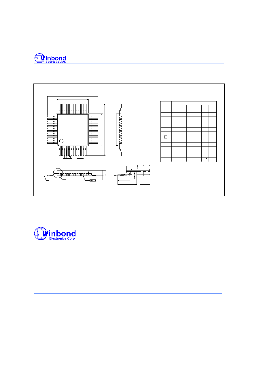
10. PACKAGE DIMENSIONS
48-pin QFP
2
1
A
H
D
D
e
b
E
H
E
y
A
A
Seating Plane
L
L
1
See Detail F
Detail F
c
37
48
1
12
13
24
25
36
1. Dimensions D & E do not include interlead
flash.
2. Dimension b does not include dambar
protrusion/intrusion.
3. Controlling dimension: Millimeters
4. General appearance spec. should be based
on final visual inspection spec.
Notes:
Symbol
Min.
Nom.
Max.
Max.
Nom.
Min.
Dimension in Inch
Dimension in mm
A
b
c
D
e
H
D
H
E
L
y
A
A
L
1
1
2
E
1.40
0.20
0.50
1.00
7.00
9.00
9.00
7.00
---
---
---
1.60
0.15
1.45
1.35
0.05
0.17
0.27
---
0.09
0.20
0.45
0.60
0.75
0.08
0
3.5
7
---
---
Headquarters
No. 4, Creation Rd. III,
Science-Based Industrial Park,
Hsinchu, Taiwan
TEL: 886-3-5770066
FAX: 886-3-5792646
http://www.winbond.com.tw/
Voice & Fax-on-demand: 886-2-27197006
Taipei Office
11F, No. 115, Sec. 3, Min-Sheng East Rd.,
Taipei, Taiwan
TEL: 886-2-27190505
FAX: 886-2-27197502
Winbond Electronics (H.K.) Ltd.
Rm. 803, World Trade Square, Tower II,
123 Hoi Bun Rd., Kwun Tong,
Kowloon, Hong Kong
TEL: 852-27513100
FAX: 852-27552064
Winbond Electronics North America Corp.
Winbond Memory Lab.
Winbond Microelectronics Corp.
Winbond Systems Lab.
2727 N. First Street, San Jose,
CA 95134, U.S.A.
TEL: 408-9436666
FAX: 408-5441798
Note: All data and specifications are subject to change without notice.
Please note that all data and specifications are subject to change without notice. All the trade marks of products
and companies mentioned in this data sheet belong to their respective owners.