
©
VITESSE
SEMICONDUCTOR CORPORATION
Page 1
11/9/99
741 Calle Plano, Camarillo, CA 93012 · 805/388-3700 · FAX: 805/987-5896
VITESSE
SEMICONDUCTOR CORPORATION
Preliminary Datasheet
VSC8131
2.488 Gbit/sec
32:1 SONET/SDH Mux with Clock Generator
G52249-0, Rev. 3.0
Features
General Description
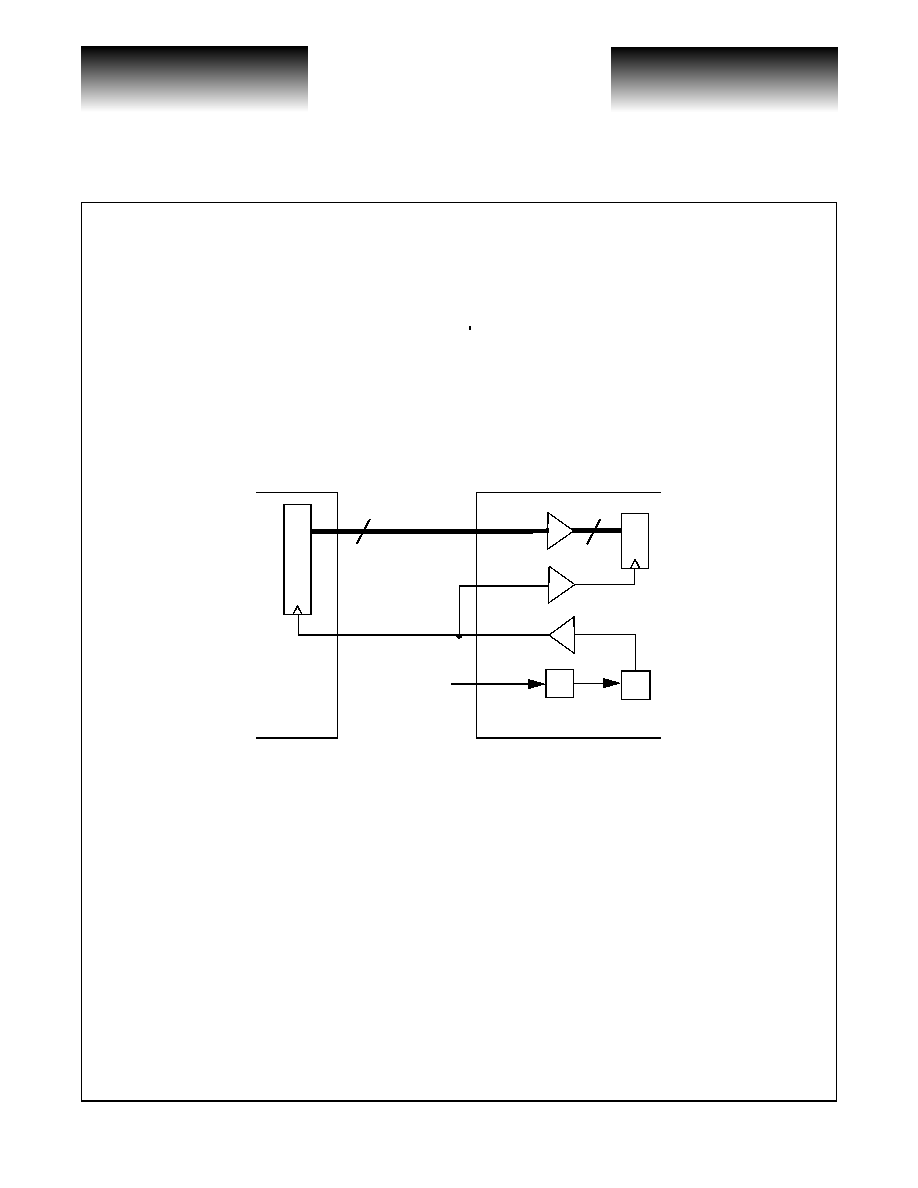
The VSC8131 multiplexes 32 TTL compatible 77.76Mb/s Parallel Data Inputs (D0-D31) into a single
LVPECL 2.488 Gb/s serial output (DO+) for use in SONET STS-48/SDH STM-16 systems. An integrated
Clock Multiplier Unit (CMU) generates a LVPECL 2.488 GHz clock signal (CO+
) from an externally supplied
LVPECL compliant 77.76MHz reference clock (REFCLK+) which is
used to retime the transmitted serialized data.
A Divide-by-32 TTL clock output (CK78OUT) is used as a clock input (CK78IN) for timing of the parallel data
inputs. Parity Checking (PARBIT) is performed on the incoming data with a selectable even or odd TTL parity mode
input (PARMODE) and a TTL Parity Error (PARERR) output. A TTL Loss Of Lock (LOL) output indicator is used to
report the loss of the REFCLK+ or for conditions resulting in the CMU losing lock to incoming clock.
VSC8131 Block DIagram
· 2.488Gb/s 32:1 Mux with Clock Generator
· SONET STS-48/SDH STM-16
· LVPECL Differential High Speed Serial Data
and Clock Outputs
· 32 TTL Parallel Data Inputs with Odd/Even
Parity Check
· 128 Pin, 14x20x2 mm Enhanced-PQFP
· Single 3.3V Supply
· 2.15W Max Power Dissipation
32:1
Multiplexer
Output
Register
PARBIT
D0
D31
Bit Rate Clock
Parallel Data
Receivers
Input
Registers
Timing
Generator
Clock/32
CMU
x32
LOL
CO+
CO-
DO+
DO-
CK78OUT
PARMODE
CK78IN
Parity
Register
PARERR
REFCLK+
REFCLK-
VITESSE
SEMICONDUCTOR CORPORATION
Preliminary Datasheet
VSC8131
2.488 Gbit/sec
32:1 SONET/SDH Mux with Clock Generator
Page 2
©
VITESSE
SEMICONDUCTOR CORPORATION
741 Calle Plano, Camarillo, CA 93012 · 805/388-3700 · FAX: 805/987-5896
11/9/99
G52249-0, Rev. 3.0
Functional Description
Low Speed Interface
The timing for the low speed parallel interface is based upon the CK78OUT output signal. The intent is to
have the device upstream from the VSC8131 use the CK78OUT clock signal as the timing source for its final
output stage latch. CK78IN is to be driven by CK78OUT, refer to Figure 1. This reduces the setup time of the
VSC8131. The maximum propagation delay permitted from CK78OUT to CK78IN is specified by
t
CKPROP
in
the AC Characteristics. The setup and hold time of the data inputs are specified with respect to the rising edge of
CK78IN. D0-D31, CK78OUT, and CK78IN are TTL compatible inputs.
Figure 1: Low Speed System Interface
Parity
A parity check is performed between the parity bit input (PARBIT) and the 32 parallel data inputs (D0-
D31). Even versus odd parity checking is selected with PARMODE. Set PARMODE low to test for odd parity.
Set PARMODE high to test for even parity. The parity error output (PARERR) is set to a logic high when a par-
ity error has occurred. The PARERR signal can be changed from an active high to active low signal by comple-
menting the PARMODE input. PARERR is re-calculated each time new parallel data is clocked in. The newly
calculated PARERR result is clocked out on the rising edge of CK78IN 2 cycles after the data is loaded. PAR-
BIT, PARMODE, and PARERR conform to TTL output levels.
CK78OUT
REFCLK
2.488 GHz
PLL
Divide by 32
VSC8131
Upstream
Device
33
33
D[0:31], PARBIT
CK78IN
©
VITESSE
SEMICONDUCTOR CORPORATION
Page 3
11/9/99
741 Calle Plano, Camarillo, CA 93012 · 805/388-3700 · FAX: 805/987-5896
VITESSE
SEMICONDUCTOR CORPORATION
Preliminary Datasheet
VSC8131
2.488 Gbit/sec
32:1 SONET/SDH Mux with Clock Generator
G52249-0, Rev. 3.0
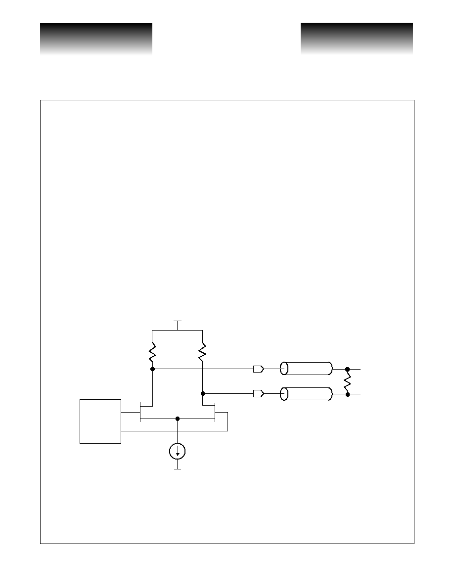
High Speed Data Output
The high speed data will be multiplexed in the sequence D0, D1 up to D31 with D0 being transmitted first.
The high speed data output driver consists of a differential pair designed to drive a 50
transmission line. The
transmission line should be terminated with a 100
resistor at the load between the true and complement out-
puts, refer to Figure 2. No connection to a termination voltage is required. The output driver is back terminated
to 50
on-chip, providing snubbing of any reflections. If used single-ended, the high speed output driver must
still be terminated differentially at the load with a 100
resistor between the true and complement output sig-
nals.
High Speed Clock Output
The high speed clock output driver consists of a differential pair designed to drive a 50
transmission line.
The transmission line should be terminated with a 100
resistor at the load between the true and complement
output, refer to Figure 2. No connection to a termination voltage is required. The output driver is back termi-
nated to 50
on-chip, providing a snubbing of any reflections. If used single-ended, the high speed output
driver must still be terminated differentially at the load with a 100
resistor between the true and complement
output signals.
Figure 2: Termination for High Speed Clock and Data Output Drivers
V
CC
V
EE
Z
0
= 50
50
100
50
Pre-Driver

VITESSE
SEMICONDUCTOR CORPORATION
Preliminary Datasheet
VSC8131
2.488 Gbit/sec
32:1 SONET/SDH Mux with Clock Generator
Page 4
©
VITESSE
SEMICONDUCTOR CORPORATION
741 Calle Plano, Camarillo, CA 93012 · 805/388-3700 · FAX: 805/987-5896
11/9/99
G52249-0, Rev. 3.0
Clock Generator
An on-chip Phase Locked Loop (PLL) generates the 2.488 GHz transmit clock from the externally provided
REFCLK input. The on-chip PLL uses a low phase noise reactance based Voltage Controlled Oscillator (VCO)
with an on-chip loop filter. The loop bandwidth of the PLL is within the SONET specified limit of 2MHz. The
REFCLK is 77.76MHz and should be of high quality. Noise on the REFCLK below the loop band width of the
PLL will pass through the PLL and appear as jitter on the output. Preconditioning of the REFCLK signal with a
VCXO may be required to avoid passing REFCLK noise with greater than 4ps RMS of jitter to the output. Such
a condition would create an output from the VSC8131 which has the REFCLK noise in addition to the intrinsic
jitter from the VSC8131 itself. REFCLK is a LVPECL level and is required to be a differential signal in order to
meet the 4pS RMS jitter spec. The true and complement inputs of the differential PECL receiver are internally
biased to VCC/2 so that the REFCLK signal can be AC coupled without using external bias resistors, refer to
Figure 3. REFCLK can be DC coupled by simply over-driving the internal bias voltage.
Figure 3: REFCLK Internal Bias Configuration
Loss of Lock
The Loss Of Lock (LOL) output is used to indicate if the CMU is locked. A loss of lock condition is
reported when the CMU does not lock to the REFCLK frequency or when the REFCLK input signal is not
present. LOL is high when the CMU is locked. LOL is low when the REFCLK input signal is not present (input
floating due to cut line or input stuck high or low). The LOL signal will appear as a pulse train of 1's and 0's
when the REFCLK is present, but the CMU is not locked to the REFCLK's frequency. The frequency of the
LOL pulse train can be anywhere from 500Hz to 50MHz.
INPUT
INPUT
V
EE
= 0V
All Resistors
3.3K
V
CC
= +3.3V
V
CC
2
V
CC
2
©
VITESSE
SEMICONDUCTOR CORPORATION
Page 5
11/9/99
741 Calle Plano, Camarillo, CA 93012 · 805/388-3700 · FAX: 805/987-5896
VITESSE
SEMICONDUCTOR CORPORATION
Preliminary Datasheet
VSC8131
2.488 Gbit/sec
32:1 SONET/SDH Mux with Clock Generator
G52249-0, Rev. 3.0
Supplies
This device is specified as a LVPECL device with a single +3.3V supply. Normal operation is to have
V
CC
=+3.3V and V
EE
=ground. Should the user desire to use the device in an ECL environment with a negative
3.3V supply, then V
CC
will be ground and V
EE
will be -3.3V. If used with V
EE
tied to -3.3V, the TTL I/O signals
are still referenced to V
EE
.
Decoupling of the power supplies is a critical element in maintaining the proper operation of the part. It is
recommended that the V
CC
power supply be decoupled using a 0.1
µ
F and 0.01
µ
F capacitor placed in parallel on
each V
CC
power supply pin as close to the package as possible. If room permits, a 0.001
µ
F capacitor should
also be placed in parallel with the 0.1
µ
F and 0.01
µ
F capacitors mentioned above. Recommended capacitors are
low inductance ceramic SMT X7R devices. For the 0.1
µ
F capacitor, a 0603 package should be used. The
0.01
µ
F and 0.001
µ
F capacitors can be either 0603 or 0403 packages.
Extra care needs to be taken when decoupling the analog power supply pins (labeled V
CCANA
). In order to
maintain the optimal jitter and loop bandwidth characteristics of the PLL contained in the VSC8131, the analog
power supply pins should be filtered from the main power supply with a 10
µ
H C-L-C pi filter. If preferred, a
ferrite bead may be used to provide the isolation. The 0.1
µ
F and 0.01
µ
F decoupling capacitors are still required
and must be connected to the supply pins between the device and the C-L-C pi filter (or ferrite bead).
For low frequency decoupling, 47
µ
F tantalum low inductance SMT caps are sprinkled over the board's
main +3.3V power supply and placed close to the C-L-C pi filter.
If the device is being used in an ECL environment with a negative 3.3V supply, then all references to decou-
pling V
CC
must be changed to V
EE
, and all references to decoupling +3.3V must be changed to -3.3V.