SUD15N06-90L
Vishay Siliconix
Document Number: 71087
S-49634--Rev. D, 20-Sep-99
www.vishay.com
S
FaxBack 408-970-5600
2-1
N-Channel 60-V (D-S), 175
_
C MOSFET, Logic Level
PRODUCT SUMMARY
V
DS
(V)
r
DS(on)
(
W
)
I
D
(A)
60
0.065 @ V
GS
= 10 V
15
60
0.090 @ V
GS
= 4.5 V
14
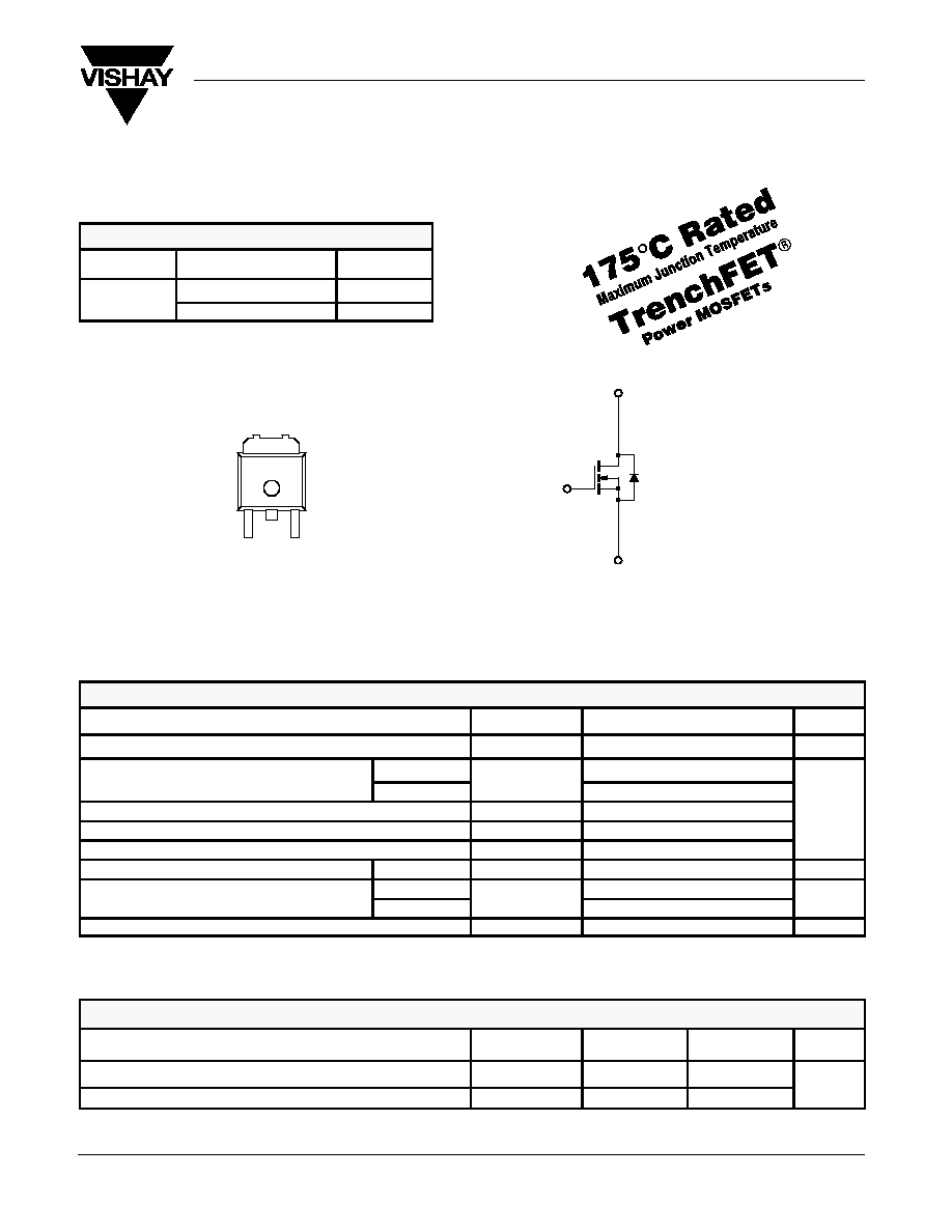
TO-252
S
G
D
Top View
Drain Connected to Tab
Order Number:
SUD15N06-90L
D
G
S
N-Channel MOSFET
ABSOLUTE MAXIMUM RATINGS (T
C
= 25_C UNLESS OTHERWISE NOTED)
Parameter
Symbol
Limit
Unit
Gate-Source Voltage
V
GS
"
20
V
Continuous Drain Current
(T
J
= 175
_
C)
T
C
= 25
_
C
I
D
15
A
Continuous Drain Current
(T
J
= 175 C)
T
C
= 100
_
C
I
D
12
A
Pulsed Drain Current
I
DM
30
A
Continuous Source Current (Diode Conduction)
I
S
15
Avalanche Current
I
AR
15
Repetitive Avalanche Energy (Duty Cycle
v
1%)
L = 0.1 mH
E
AR
11
mJ
Maximum Power Dissipation
T
C
= 25
_
C
P
D
37
W
Maximum Power Dissipation
T
A
= 25
_
C
P
D
2
a
W
Operating Junction and Storage Temperature Range
T
J
, T
stg
Ł55 to 175
_
C
THERMAL RESISTANCE RATINGS
Parameter
Symbol
Typical
Maximum
Unit
Junction-to-Ambient Free Air, FR4 Board Mount
a
R
thJA
60
70
_
C/W
Junction-to-Case
R
thJC
3.7
4.0
_
C/W
Notes:
a.
1.36 x 2.1 surface mounted on 1" x 1" FR4 Board.

SUD15N06-90L
Vishay Siliconix
www.vishay.com
S
FaxBack 408-970-5600
2-2
Document Number: 71087
S-49634--Rev. D, 20-Sep-99
SPECIFICATIONS (T
J
= 25_C UNLESS OTHERWISE NOTED)
Parameter
Symbol
Test Condition
Min
Typ
a
Max
Unit
Static
Drain-Source Breakdown Voltage
V
(BR)DSS
V
GS
= 0 V, I
D
= 250
m
A
60
V
Gate Threshold Voltage
V
GS(th)
V
DS
= V
GS
, I
D
= 250
m
A
1.0
2.0
3.0
V
Gate-Body Leakage
I
GSS
V
DS
= 0 V, V
GS
=
"
20 V
"
100
nA
Z
G
V l
D i C
I
V
DS
= 60 V, V
GS
= 0 V
1
A
Zero Gate Voltage Drain Current
I
DSS
V
DS
= 60 V, V
GS
= 0 V, T
J
= 125
_
C
50
m
A
V
DS
= 60 V, V
GS
= 0 V, T
J
= 175
_
C
150
On-State Drain Current
b
I
D(on)
V
DS
= 5 V, V
GS
= 10 V
15
A
D i S
O S
R
i
b
V
GS
= 10 V, I
D
= 10 A
0.050
0.065
W
Drain Source On State Resistance
b
r
DS(
)
V
GS
= 10 V, I
D
= 10 A, T
J
= 125
_
C
0.12
W
Drain-Source On-State Resistance
b
r
DS(on)
V
GS
= 10 V, I
D
= 10 A, T
J
= 175
_
C
0.15
W
V
GS
= 4.5 V, I
D
= 5 A
0.065
0.090
Forward Transconductance
b
g
fs
V
DS
= 15 V, I
D
= 10 A
11
S
Dynamic
Input Capacitance
C
iss
V
0 V V
25 V f
1 MH
524
F
Output Capacitance
C
oss
V
GS
= 0 V, V
DS
= 25 V, f = 1 MHz
98
pF
Reverse Transfer Capacitance
C
rss
28
Total Gate Charge
c
Q
g
V
30 V V
10 V I
15 A
12
20
C
Gate-Source Charge
c
Q
gs
V
DS
= 30 V, V
GS
= 10 V, I
D
= 15 A
2
nC
Gate-Drain Charge
c
Q
gd
3.5
Turn-On Delay Time
c
t
d(on)
V
30 V R
2
W
7
20
Rise Time
c
t
r
V
DD
= 30 V, R
L
= 2
W
I
15 A V
10 V R
2 5
W
8
25
ns
Turn-Off Delay Time
c
t
d(off)
DD
,
L
I
D
^
15 A, V
GEN
= 10 V, R
G
= 2.5
W
15
40
ns
Fall Time
c
t
f
7
20
Source-Drain Diode Ratings and Characteristics (T
C
= 25
_
C)
Pulsed Current
I
SM
30
A
Diode Forward Voltage
V
SD
I
F
= 15 A, V
GS
= 0 V
0.9
1.2
V
Reverse Recovery Time
t
rr
I
F
= 15 A, di/dt = 100 A/
m
s
29
60
ns
Notes:
a.
For design aid only; not subject to production testing.
b.
Pulse test; pulse width
v
300
m
s, duty cycle
v
2%.
c.
Independent of operating temperature.
SUD15N06-90L
Vishay Siliconix
Document Number: 71087
S-49634--Rev. D, 20-Sep-99
www.vishay.com
S
FaxBack 408-970-5600
2-3
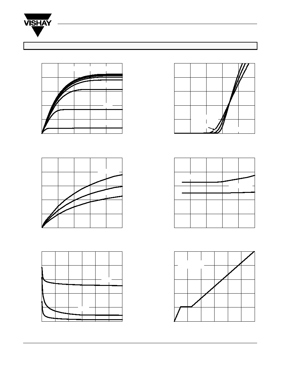
TYPICAL CHARACTERISTICS (25_C UNLESS NOTED)
Output Characteristics
Transfer Characteristics
Capacitance
Gate Charge
Transconductance
On-Resistance vs. Drain Current
V
DS
Ł Drain-to-Source Voltage (V)
Ł Drain Current (A)
I
D
V
GS
Ł Gate-to-Source Voltage (V)
Ł Drain Current (A)
I
D
Ł Gate-to-Source V
oltage
(V)
Ł On-Resistance (
Q
g
Ł Total Gate Charge (nC)
I
D
Ł Drain Current (A)
V
DS
Ł Drain-to-Source Voltage (V)
C Ł Capacitance (pF)
r DS(on)
W
)
V
GS
Ł T
ransconductance
(S)
g
fs
0
10
20
30
40
50
0
2
4
6
8
10
0
4
8
12
16
20
0
4
8
12
16
20
24
0
5
10
15
20
25
0
4
8
12
16
20
0
0.02
0.04
0.06
0.08
0.10
0
4
8
12
16
20
0
4
8
12
16
20
0
1
2
3
4
5
25
_
C
Ł55
_
C
T
C
= 125
_
C
V
DS
= 30 V
I
D
= 15 A
V
GS
= 10 thru 6 V
V
GS
= 4.5 V
C
rss
T
C
= Ł55
_
C
25
_
C
125
_
C
3 V
4 V
5 V
V
GS
= 10 V
0
200
400
600
800
1000
0
10
20
30
40
50
60
C
iss
C
oss
I
D
Ł Drain Current (A)

SUD15N06-90L
Vishay Siliconix
www.vishay.com
S
FaxBack 408-970-5600
2-4
Document Number: 71087
S-49634--Rev. D, 20-Sep-99
TYPICAL CHARACTERISTICS (25_C UNLESS NOTED)
0
0.3
0.6
0.9
1.2
On-Resistance vs. Junction Temperature
Source-Drain Diode Forward Voltage
(Normalized)
Ł On-Resistance (
T
J
Ł Junction Temperature (
_
C)
V
SD
Ł Source-to-Drain Voltage (V)
r DS(on)
W
)
Ł Source Current (A)
I
S
0
0.5
1.0
1.5
2.0
2.5
Ł50
Ł25
0
25
50
75
100
125
150
175
100
10
1
V
GS
= 10 V
I
D
= 10 A
T
J
= 25
_
C
T
J
= 150
_
C
THERMAL RATINGS
Drain Current vs. Case Temperature
Normalized Thermal Transient Impedance, Junction-to-Case
Square Wave Pulse Duration (sec)
2
1
0.1
0.01
10
Ł4
10
Ł3
10
Ł2
10
Ł1
Normalized Ef
fective
T
ransient
Thermal Impedance
3
Safe Operating Area
T
C
Ł Case Temperature (
_
C)
V
DS
Ł Drain-to-Source Voltage (V)
Ł Drain Current (A)
I D
Ł Drain Current (A)
ID
50
10
0.1
0
4
8
12
16
20
0
25
50
75
100
125
150
175
0.2
0.1
0.05
0.02
Single Pulse
Duty Cycle = 0.5
0.1
1
10
100
1
1
T
C
= 25
_
C
Single Pulse
1 ms
10 ms
100 ms
dc
100
m
s
10
m
s
Limited
by r
DS(on)