SMF5V0A to SMF51A
Document Number 85811
Rev. 2.0, 29-Apr-05
Vishay Semiconductors
www.vishay.com
1
17249
Surface Mount ESD Protection Diodes
Features
· For surface mounted applications
· Low-profile package
· Optimized for LAN protection applications
· Ideal for ESD protection of data lines in
accordance with IEC 61000-4-2 (IEC801-2)
· Ideal for EFT protection of data lines in
accordance with IEC 61000-4-4 (IEC801-4)
· IEC 61000-4-2 (ESD) 15 kV (air) 8 kV (contact)
· Low incremental surge resistance, excellent
clamping capability
· 200 W peak pulse power capability with a
10/1000
µs waveform, repetition rate
(duty cycle): 0.01 %
· Very fast response time
· High temperature soldering guaranteed:
260 °C/ 10 seconds at terminals
· Lead (Pb)-free component
· Component in accordance to RoHS 2002/95/EC
and WEEE 2002/96/EC
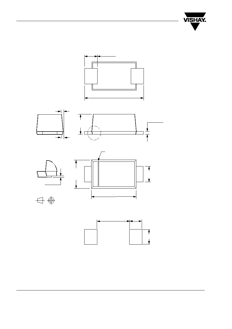
Mechanical Data
Case: JEDEC DO-219AB (SMF
®
) Plastic case
Terminals: Solder plated, solderable per
MIL-STD-750, Method 2026
Polarity:The band denotes the cathode, which is
positive with respect to the anode under normal
TVS operation
Mounting Position: Any
Weight: approx. 15 mg
Packaging Codes/Options:
GS18 / 10 k per 13 " reel (8 mm tape), 50 k/box
GS08 / 3 k per 7 " reel (8 mm tape), 30 k/box
Absolute Maximum Ratings
Ratings at 25 °C, ambient temperature unless otherwise specified
1)
Non-repetitive current pulse and derated above T
A
= 25 °C
Thermal Characteristics
Ratings at 25 °C, ambient temperature unless otherwise specified
2) Mounted on epoxy glass PCB with 3 x 3 mm, Cu pads (
40 µm thick)
Parameter
Test condition
Symbol
Value
Unit
Peak pulse power dissipation
10/1000
µs waveform
1)
P
PPM
200
W
8/20
µs waveform
1)
P
PPM
1000
W
Peak pulse current
10/1000
µs waveform
1)
I
PPM
next
Table
A
Peak forward surge current
8.3 ms single half sine-wave
I
FSM
20
A
Parameter
Test condition
Symbol
Value
Unit
Thermal resistance
2)
R
thJA
180
K/W
Operation junction and storage
temperature range
T
stg
, T
J
- 55 to + 150
°C
e3
SMF5V0A to SMF51A
Document Number 85811
Rev. 2.0, 29-Apr-05
Vishay Semiconductors
www.vishay.com
3
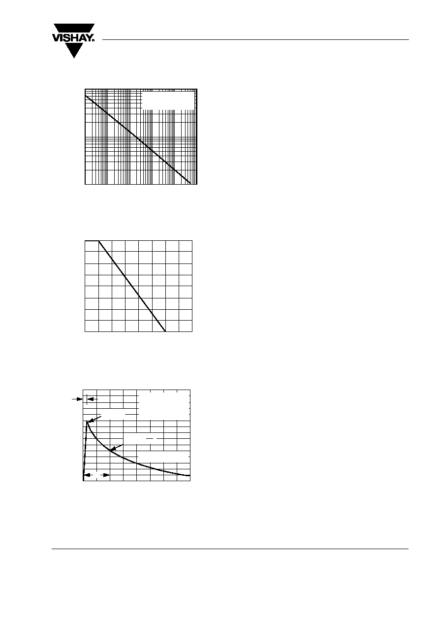
Typical Characteristics (Tamb = 25
°C unless otherwise specified)
Figure 1. Peak Pulse Power Rating
Figure 2. Pulse Derating Curve
Figure 3. Pulse Waveform
P
PPM
-
Peak
Pulse
Power
(kW)
0.1
1
10
0.1
µs
1.0
µs
10
µs
t
d
- Pulse Width (sec.)
100
µs
1.0ms
10ms
Non-repetitive Pulse
Waveform shown in Fig. 3
T
A
= 25 °C
17250
0
25
50
75
100
0
75
25
50
100
125
150
175
200
Peak
Pulse
Power
(P
PP
)
o
r
C
urrent
(I
PPM
)
Derating
i
n
Percentage,
%
T
A
- Ambient Temperature (°C)
17251
0
50
100
150
I
PPM
-
Peak
Pulse
C
urrent,
%
I
RSM
T
J
= 25 °C
Pulse Width (td)
is defined as the point
where the peak current
decays to 50% of I
PPM
tr = 10
µs
Peak Value
I
PPM
Half Value - IPP
I
PPM
2
td
10/1000 sec. Waveform
as defined by R.E.A.
0
1.0
2.0
3.0
4.0
t - Time (ms)
17252