SMB10J5.0 thru 40A and SMB8J5.0C thru 40CA
Vishay Semiconductors
formerly General Semiconductor
Document Number 88422
www.vishay.com
11-Mar-04
1
New Product
High Power Density Surface Mount T
RANS
Z
ORB
®
Transient Voltage Suppressors
Stand-off Voltage 5.0 to 40V
Peak Pulse Power 1000W (unidirectional)
800W (bidirectional)
Devices for Bidirectional Applications
For bi-directional devices, use suffix C or CA (e.g. SMB8J10CA). Electrical characteristics apply in both directions.
Maximum Ratings & Thermal Characteristics
Ratings at 25°C ambient temperature unless otherwise specified.
Parameter
Symbol
Value
Unit
Peak pulse power dissipation with
unidirectional
P
PPM
1000
W
a 10/1000µs waveform
(1,2)
(see fig. 1)
bidirectional
800
Peak pulse current with a 10/1000µs waveform
(1)
I
PPM
See Next Table
A
Peak forward surge current 8.3ms single half sine-wave
I
FSM
100
A
uni-directional only
(2)
Typical thermal resistance, junction to ambient
(3)
R
JA
72 °C/W
Typical thermal resistance, junction to lead
R
JL
20 °C/W
Operating junction and storage temperature range
T
J
, T
STG
55 to +150
°C
Notes: (1) Non-repetitive current pulse, per Fig. 3 and derated above T
A
= 25°C per Fig. 2
(2) Mounted on 0.2 x 0.2" (5.0 x 5.0mm) copper pads to each terminal
(3) Mounted on minimum recommended pad layout
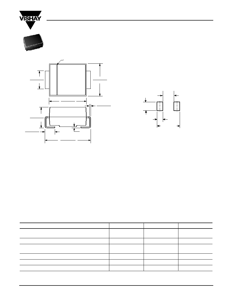
0.180 (4.57)
0.160 (4.06)
0.012 (0.305)
0.006 (0.152)
0.008
(0.203)
Max.
0.220 (5.59)
0.205 (5.21)
0.060 (1.52)
0.030 (0.76)
0.155 (3.94)
0.130 (3.30)
0.086 (2.20)
0.077 (1.95)
0.096 (2.44)
0.084 (2.13)
Cathode Band
Dimensions in inches
and (millimeters)
DO-214AA (SMB)
Features
· 1000W for unidirectional and 800W for bidirectional
peak pulse power capability with a 10/1000µs
waveform, repetition rate (duty cycle): 0.01%
· Plastic package has Underwriters Laboratory
Flammability Classification 94V-0
· Low profile package with built-in strain relief for
surface mounted applications
· Glass passivated junction
· Low incremental surge resistance,
excellent clamping capability
· Very fast response time
Mechanical Data
Case: JEDEC DO-214AA molded plastic over
passivated chip
Terminals: Solder plated, solderable per MIL-STD-750,
Method 2026
High temperature soldering guaranteed:
250°C/10 seconds at terminals
Polarity: For uni-directional types the band denotes the
cathode, which is positive with respect to the anode
under normal TVS operation
Mounting Position: Any Weight: 0.003oz., 0.093g
0.085 MAX
(2.16 MAX)
0.060 MIN
(1.52 MIN)
0.220 REF
0.086 MIN
(2.20 MIN)
Mounting Pad Layout

SMB10J5.0 thru 40A and SMB8J5.0C thru 40CA
Vishay Semiconductors
formerly General Semiconductor
www.vishay.com
Document Number 88422
2
11-Mar-04
Unidirectional
Electrical Characteristics
Ratings at 25°C ambient temperature unless otherwise specified. V
F
= 3.5V at I
F
= 50A (uni-directional only)
Breakdown
Maximum
Maximum
Maximum
Device Type
Device
Voltage
Test
Stand-off
Reverse Leakage Peak Pulse Surge
Clamping
Marking
V
(BR)
(V)
(1)
Current
Voltage
at V
WM
Current I
PPM
Voltage at I
PPM
Code
Min
Max
at I
T
(mA)
V
WM
(V)
I
D
(µA)
(A)
(2)
V
C
(V)
SMB10J5.0
1AD
6.40
7.82
10
5.0
1000
104.2
9.6
SMB10J5.0A
1AE
6.40
7.07
10
5.0
1000
108.7
9.2
SMB10J6.0
1AF
6.67
8.15
10
6.0
1000
87.7
11.4
SMB10J6.0A
1AG
6.67
7.37
10
6.0
1000
97.1
10.3
SMB10J6.5
1AH
7.22
8.82
10
6.5
500
81.3
12.3
SMB10J6.5A
1AK
7.22
7.98
10
6.5
500
89.3
11.2
SMB10J7.0
1AL
7.78
9.51
10
7.0
200
75.2
13.3
SMB10J7.0A
1AM
7.78
8.60
10
7.0
200
83.3
12.0
SMB10J7.5
1AN
8.33
10.2
1.0
7.5
100
69.9
14.3
SMB10J7.5A
1AP
8.33
9.21
1.0
7.5
100
77.5
12.9
SMB10J8.0
1AQ
8.89
10.9
1.0
8.0
50
66.7
15.0
SMB10J8.0A
1AR
8.89
9.83
1.0
8.0
50
73.5
13.6
SMB10J8.5
1AS
9.44
11.5
1.0
8.5
20
62.9
15.9
SMB10J8.5A
1AT
9.44
10.4
1.0
8.5
20
69.4
14.4
SMB10J9.0
1AU
10.0
12.2
1.0
9.0
10
59.2
16.9
SMB10J9.0A
1AV
10.0
11.1
1.0
9.0
10
64.9
15.4
SMB10J10
1AW
11.1
13.6
1.0
10
5.0
53.2
18.8
SMB10J10A
1AX
11.1
12.3
1.0
10
5.0
58.8
17.0
SMB10J11
1AY
12.2
14.9
1.0
11
5.0
49.8
20.1
SMB10J11A
1AZ
12.2
13.5
1.0
11
5.0
54.9
18.2
SMB10J12
1BD
13.3
16.3
1.0
12
5.0
45.5
22.0
SMB10J12A
1BE
13.3
14.7
1.0
12
5.0
50.3
19.9
SMB10J13
1BF
14.4
17.6
1.0
13
1.0
42.0
23.8
SMB10J13A
1BG
14.4
15.9
1.0
13
1.0
46.5
21.5
SMB10J14
1BH
15.6
19.1
1.0
14
1.0
38.8
25.8
SMB10J14A
1BK
15.6
17.2
1.0
14
1.0
43.1
23.2
SMB10J15
1BL
16.7
20.4
1.0
15
1.0
37.2
26.9
SMB10J15A
1BM
16.7
18.5
1.0
15
1.0
41.0
24.4
SMB10J16
1BN
17.8
21.8
1.0
16
1.0
34.7
28.8
SMB10J16A
1BP
17.8
19.7
1.0
16
1.0
38.5
26.0
SMB10J17
1BQ
18.9
23.1
1.0
17
1.0
32.8
30.5
SMB10J17A
1BR
18.9
20.9
1.0
17
1.0
36.2
27.6
SMB10J18
1BS
20.0
24.4
1.0
18
1.0
31.1
32.2
SMB10J18A
1BT
20.0
22.1
1.0
18
1.0
34.2
29.2
SMB10J20
1BU
22.2
27.1
1.0
20
1.0
27.9
35.8
SMB10J20A
1BV
22.2
24.5
1.0
20
1.0
30.9
32.4
SMB10J22
1BW
24.4
29.8
1.0
22
1.0
25.4
39.4
SMB10J22A
1BX
24.4
26.9
1.0
22
1.0
28.2
35.5
SMB10J24
1BY
26.7
32.6
1.0
24
1.0
23.3
43.0
SMB10J24A
1BZ
26.7
29.5
1.0
24
1.0
25.7
38.9
SMB10J26
1CD
28.9
35.3
1.0
26
1.0
21.5
46.6
SMB10J26A
1CE
28.9
31.9
1.0
26
1.0
23.8
42.1
SMB10J28
1CF
31.1
38.0
1.0
28
1.0
20.0
50.0
SMB10J28A
1CG
31.1
34.4
1.0
28
1.0
22.0
45.4
SMB10J30
1CH
33.3
40.7
1.0
30
1.0
18.7
53.5
SMB10J30A
1CK
33.3
36.8
1.0
30
1.0
20.7
48.4
Notes: (1) V
(BR)
measured after I
T
applied for 300µs square wave pulse or equivalent
(2) Surge current waveform per Fig. 3 and derate per Fig. 2
(3) All terms and symbols are consistent with ANSI/IEEE C62.35

SMB10J5.0 thru 40A and SMB8J5.0C thru 40CA
Vishay Semiconductors
formerly General Semiconductor
Document Number 88422
www.vishay.com
11-Mar-04
3
Unidirectional
Electrical Characteristics
Ratings at 25°C ambient temperature unless otherwise specified. V
F
= 3.5V at I
F
= 50A (uni-directional only)
Breakdown
Maximum
Maximum
Maximum
Device Type
Device
Voltage
Test
Stand-off
Reverse Leakage Peak Pulse Surge
Clamping
Marking
V
(BR)
(V)
(1)
Current
Voltage
at V
WM
Current I
PPM
Voltage at I
PPM
Code
Min
Max
at I
T
(mA)
V
WM
(V)
I
D
(µA)
(A)
(2)
V
C
(V)
SMB10J33
1CL
36.7
44.9
1.0
33
1.0
16.9
59.0
SMB10J33A
1CM
36.7
40.6
1.0
33
1.0
18.8
53.3
SMB10J36
1CN
40.0
48.9
1.0
36
1.0
15.6
64.3
SMB10J36A
1CP
40.0
44.2
1.0
36
1.0
17.2
58.1
SMB10J40
1CQ
44.4
54.3
1.0
40
1.0
14.0
71.4
SMB10J40A
1CR
44.4
49.1
1.0
40
1.0
15.5
64.5
Notes: (1) V
(BR)
measured after I
T
applied for 300µs square wave pulse or equivalent
(2) Surge current waveform per Fig. 3 and derate per Fig. 2
(3) All terms and symbols are consistent with ANSI/IEEE C62.35
SMB10J5.0 thru 40A and SMB8J5.0C thru 40CA
Vishay Semiconductors
formerly General Semiconductor
www.vishay.com
Document Number 88422
4
11-Mar-04
Bidirectional
Electrical Characteristics
Ratings at 25°C ambient temperature unless otherwise specified.
Breakdown
Maximum
Maximum
Maximum
Device Type
Device
Voltage
Test
Stand-off
Reverse Leakage Peak Pulse Surge
Clamping
Marking
V
(BR)
(V)
(1)
Current
Voltage
at V
WM
Current I
PPM
Voltage at I
PPM
Code
Min
Max
at I
T
(mA)
V
WM
(V)
I
D
(µA)
(3)
(A)
(2)
V
C
(V)
SMB8J5.0C
1AD
6.40
7.82
10
5.0
2000
83.3
9.6
SMB8J5.0CA
1AE
6.40
7.25
10
5.0
2000
87.0
9.2
SMB8J6.0C
1AF
6.67
8.15
10
6.0
2000
70.2
11.4
SMB8J6.0CA
1AG
6.67
7.37
10
6.0
2000
77.7
10.3
SMB8J6.5C
1AH
7.22
8.82
10
6.5
1000
65.0
12.3
SMB8J6.5CA
1AK
7.22
7.98
10
6.5
1000
71.4
11.2
SMB8J7.0C
1AL
7.78
9.51
10
7.0
400
60.2
13.3
SMB8J7.0CA
1AM
7.78
8.60
10
7.0
400
66.7
12.0
SMB8J7.5C
1AN
8.33
10.2
1.0
7.5
200
55.9
14.3
SMB8J7.5CA
1AP
8.33
9.21
1.0
7.5
200
62.0
12.9
SMB8J8.0C
1AQ
8.89
10.9
1.0
8.0
100
53.3
15.0
SMB8J8.0CA
1AR
8.89
9.83
1.0
8.0
100
58.8
13.6
SMB8J8.5C
1AS
9.44
11.5
1.0
8.5
40
50.3
15.9
SMB8J8.5CA
1AT
9.44
10.4
1.0
8.5
40
55.6
14.4
SMB8J9.0C
1AU
10.0
12.2
1.0
9.0
20
47.3
16.9
SMB8J9.0CA
1AV
10.0
11.1
1.0
9.0
20
51.9
15.4
SMB8J10C
1AW
11.1
13.6
1.0
10
10
42.6
18.8
SMB8J10CA
1AX
11.1
12.3
1.0
10
10
47.1
17.0
SMB8J11C
1AY
12.2
14.9
1.0
11
5.0
39.8
20.1
SMB8J11CA
1AZ
12.2
13.5
1.0
11
5.0
44.0
18.2
SMB8J12C
1BD
13.3
16.3
1.0
12
5.0
36.4
22.0
SMB8J12CA
1BE
13.3
14.7
1.0
12
5.0
40.2
19.9
SMB8J13C
1BF
14.4
17.6
1.0
13
1.0
33.6
23.8
SMB8J13CA
1BG
14.4
15.9
1.0
13
1.0
37.2
21.5
SMB8J14C
1BH
15.6
19.1
1.0
14
1.0
31.0
25.8
SMB8J14CA
1BK
15.6
17.2
1.0
14
1.0
34.5
23.2
SMB8J15C
1BL
16.7
20.4
1.0
15
1.0
29.7
26.9
SMB8J15CA
1BM
16.7
18.5
1.0
15
1.0
32.8
24.4
SMB8J16C
1BN
17.8
21.8
1.0
16
1.0
27.8
28.8
SMB8J16CA
1BP
17.8
19.7
1.0
16
1.0
30.8
26.0
SMB8J17C
1BQ
18.9
23.1
1.0
17
1.0
26.2
30.5
SMB8J17CA
1BR
18.9
20.9
1.0
17
1.0
29.0
27.6
SMB8J18C
1BS
20.0
24.4
1.0
18
1.0
24.8
32.2
SMB8J18CA
1BT
20.0
22.1
1.0
18
1.0
27.4
29.2
SMB8J20C
1BU
22.2
27.1
1.0
20
1.0
22.3
35.8
SMB8J20CA
1BV
22.2
24.5
1.0
20
1.0
24.7
32.4
SMB8J22C
1BW
24.4
29.8
1.0
22
1.0
20.3
39.4
SMB8J22CA
1BX
24.4
26.9
1.0
22
1.0
22.5
35.5
SMB8J24C
1BY
26.7
32.6
1.0
24
1.0
18.6
43.0
SMB8J24CA
1BZ
26.7
29.5
1.0
24
1.0
20.6
38.9
SMB8J26C
1CD
28.9
35.3
1.0
26
1.0
17.2
46.6
SMB8J26CA
1CE
28.9
31.9
1.0
26
1.0
19.0
42.1
SMB8J28C
1CF
31.1
38.0
1.0
28
1.0
16.0
50.0
SMB8J28CA
1CG
31.1
34.4
1.0
28
1.0
17.6
45.4
SMB8J30C
1CH
33.3
40.7
1.0
30
1.0
15.0
53.5
SMB8J30CA
1CK
33.3
36.8
1.0
30
1.0
16.5
48.4
Notes: (1) V
(BR)
measured after I
T
applied for 300µs square wave pulse or equivalent
(2) Surge current waveform per Fig. 3 and derate per Fig. 2
(3) All terms and symbols are consistent with ANSI/IEEE C62.35

SMB10J5.0 thru 40A and SMB8J5.0C thru 40CA
Vishay Semiconductors
formerly General Semiconductor
Document Number 88422
www.vishay.com
11-Mar-04
5
Bidirectional
Electrical Characteristics
Ratings at 25°C ambient temperature unless otherwise specified.
Breakdown
Maximum
Maximum
Maximum
Device Type
Device
Voltage
Test
Stand-off
Reverse Leakage Peak Pulse Surge
Clamping
Marking
V
(BR)
(V)
(1)
Current
Voltage
at V
WM
Current I
PPM
Voltage at I
PPM
Code
Min
Max
at I
T
(mA)
V
WM
(V)
I
D
(µA)
(3)
(A)
(2)
V
C
(V)
SMB8J33C
1CL
36.7
44.9
1.0
33
1.0
13.6
59.0
SMB8J33CA
1CM
36.7
40.6
1.0
33
1.0
15.0
53.3
SMB8J36C
1CN
40.0
48.9
1.0
36
1.0
12.4
64.3
SMB8J36CA
1CP
40.0
44.2
1.0
36
1.0
13.8
58.1
SMB8J40C
1CQ
44.4
54.3
1.0
40
1.0
11.2
71.4
SMB8J40CA
1CR
44.4
49.1
1.0
40
1.0
12.4
64.5
Notes: (1) V
(BR)
measured after I
T
applied for 300µs square wave pulse or equivalent
(2) Surge current waveform per Fig. 3 and derate per Fig. 2
(3) All terms and symbols are consistent with ANSI/IEEE C62.35