Si9183
Vishay Siliconix
Document Number: 71258
S-40593--Rev. E, 29-Mar-04
www.vishay.com
1
High-Performance, Size Saving 150-mA CMOS LDO Regulator
FEATURES
D Low 135-mV Dropout at 150-mA Load
D Guaranteed 150-mA Output Current
D 300-mA Peak Output Current Capability
D Uses Low ESR Ceramic Output Capacitor
D Fast Load And Line Transient Response
D Low Output Noise
D 1-mA Maximum Shutdown Current
D Built-in Short Circuit And Thermal Protection
D Fixed 1.5-V, 1.8-V, 2.0-V, 2.5-V, 2.7-V, 2.8-V, 2.85-V,
3.0-V, 3.3-V, 3.6-V, 5.0-V or Adjustable Output
Voltage Options (Version B)
D Thin SOT-23 5-Pin Package
APPLICATIONS
D Battery Powered Portable Systems
D Cellular Phones
D PDAs, Palmtops
D Pagers
D Post Regulators for Multi-Output Converters
D Notebook Computers
DESCRIPTION
The Si9183 is a high performance yet size saving 150-mA
CMOS LDO (low dropout) voltage regulator. Its ultra low
ground current and dropout voltage prolong battery life in
portable electronics. The device provides LINE/LOAD
transient response and ripple rejection superior to that of
Bipolar or BiCMOS LDO regulators. It is designed to maintain
regulation while delivering 300-mA peak current. The Si9183
drives lower cost ceramic, as well as tantalum, output
capacitors. Stability is guaranteed from maximum load current
down to 0-mA load. An external noise bypass capacitor
connected to the device's C
BP
pin will reduce the LDO's
self-noise for low noise applications. The Si9183 includes a
shutdown feature that allows users to completely disable the
device and save power when no output is required.
The Si9183, in Thin SOT23-5 packaging, is available in two
versions (Version A or B). Version A offers low noise
performance, while Version B features adjustable output
voltage.
The Si9183 is available in both standard and lead (Pb)-free
packages.
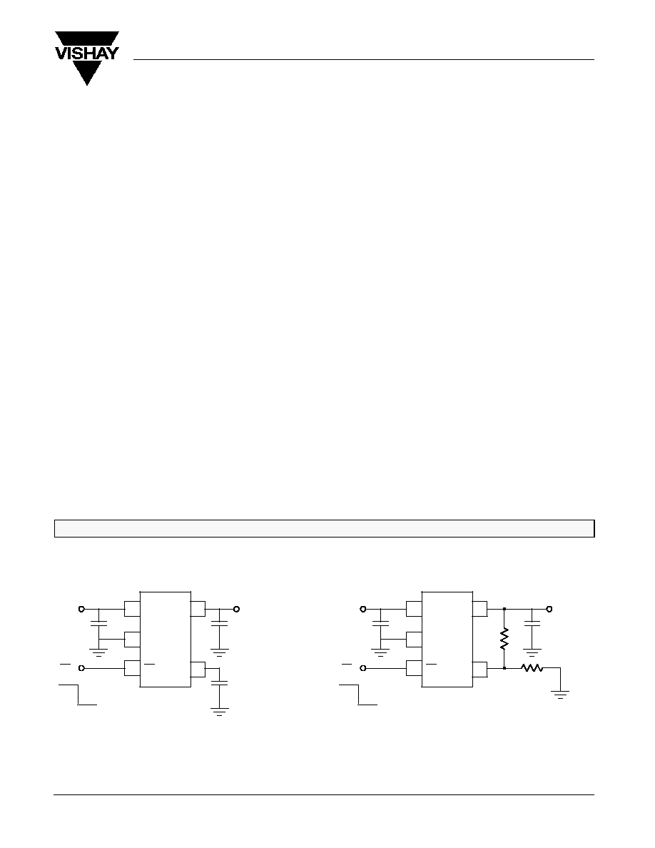
TYPICAL APPLICATIONS CIRCUITS
FIGURE 1. Version A with Low Output Noise
FIGURE 2. Version B with Adjustable Output
3
2
Si9183-A
1
4
5
V
IN
GND
SD
V
OUT
BP
V
IN
SD
V
OUT
1 mF
2.2 mF
Thin SOT-23, 5-Lead
3
2
Si9183-B
1
4
5
V
IN
GND
SD
V
OUT
FB
V
IN
SD
V
OUT
1 mF
2.2 mF
0.1 mF
ON
OFF
ON
OFF
Thin SOT-23, 5-Lead

Si9183
Vishay Siliconix
www.vishay.com
2
Document Number: 71258
S-40593--Rev. E, 29-Mar-04
ABSOLUTE MAXIMUM RATINGS
Input Voltage, V
IN
6.5 V
. . . . . . . . . . . . . . . . . . . . . . . . . . . . . . . . . . . . . . . . . . . .
SD Input Voltage, V
SD
-0.3 V to V
IN
. . . . . . . . . . . . . . . . . . . . . . . . . . . . . . . . .
Output Current, I
OUT
Short Circuit Protected
. . . . . . . . . . . . . . . . . . . . . . . . . .
Output Voltage, V
OUT
-0.3 V to V
O(nom)
+ 0.3 V
. . . . . . . . . . . . . . . . . . . . . . . .
Maximum Junction Temperature, T
J(max)
150_C
. . . . . . . . . . . . . . . . . . . . . . .
Storage Temperature, T
STG
-65_C to 125_C
. . . . . . . . . . . . . . . . . . . . . . . . . .
ESD (Human Body Model)
2 kV
. . . . . . . . . . . . . . . . . . . . . . . . . . . . . . . . . . . . .
Power Dissipation (Package)
a
, b
5-Pin SOT-23
555 mW
. . . . . . . . . . . . . . . . . . . . . . . . . . . . . . . . . . . . . . . . . . . .
Thermal Impedance (Q
JA
)
5-Pin SOT-23
180 _C/W
. . . . . . . . . . . . . . . . . . . . . . . . . . . . . . . . . . . . . . . . . . .
Notes
a.
Device mounted with all leads soldered or welded to multi-layer (1S2P)
JEDEC board, horizontal orientation.
b.
Derate 5.5 mW/_C above T
A
= 25_C.
Stresses beyond those listed under "Absolute Maximum Ratings" may cause permanent damage to the device. These are stress ratings only, and functional operation
of the device at these or any other conditions beyond those indicated in the operational sections of the specifications is not implied. Exposure to absolute maximum rating
conditions for extended periods may affect device reliability.
RECOMMENDED OPERATING RANGE
Input Voltage, V
IN
2 V to 6 V
. . . . . . . . . . . . . . . . . . . . . . . . . . . . . . . . . . . . . . . .
Output Voltage, V
OUT
(Adjustable Version)
1.5 V to 5 V
. . . . . . . . . . . . . . . . . .
SD Input Voltage, V
SD
0 V to V
IN
. . . . . . . . . . . . . . . . . . . . . . . . . . . . . . . . . . . .
Operating Ambient Temperature, T
A
-40_C to 85_C
. . . . . . . . . . . . . . . . . . . .
Operating Junction Temperature, T
J
-40_C to 125_C
. . . . . . . . . . . . . . . . . . .
C
IN
= 1
m
F, C
OUT
= 2.2
m
F (ceramic, X5R or X7R type) , C
BP
= 0.1
m
F (ceramic)
C
OUT
Range = 1
m
F to 10
m
F (
"
20% tolerance,
"
20% over temperature; ESR = 0.4 to 4
W
at dc to 100 kHz, 0 t0 0.4
W
> 100 kHz) )
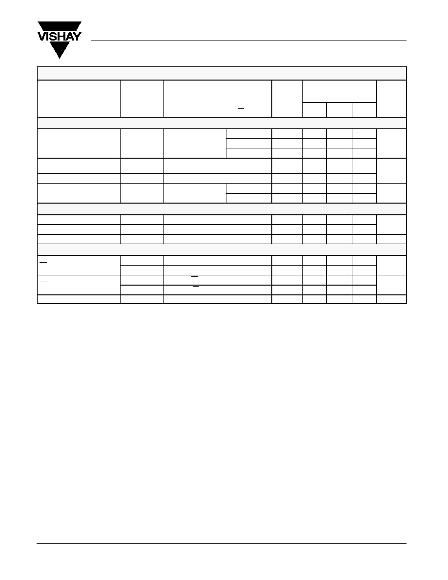
SPECIFICATIONS (T
A
= 25_C)
Test Conditions
Unless Otherwise Specified
V V
1 V I
1 A
Limits
-40 to 85_C
Parameter
Symbol
V
IN
= V
OUT(nom)
+ 1 V, I
OUT
= 1 mA
C
IN
= 1 mF, C
OUT
= 2.2 mF, V
SD
= 1.5 V
Temp
a
Min
b
Typ
c
Max
b
Unit
Input Voltage Range
V
IN
Full
2
6
V
Output Voltage Range
Adjustable Version
Full
1.5
5
V
Output Voltage Accuracy
V
OUT
1 mA v I
OUT
v 150 mA
Room
-1.5
1.5
% V
O(
)
Output Voltage Accuracy
(Fixed Versions)
OUT
1 mA v I
OUT
v 150 mA
Full
-2.5
2.5
% V
O(nom)
Feedback Voltage (ADJ version)
V
FB
Room
1.188
1.215
1.240
V
Feedback Voltage (ADJ version)
V
FB
Full
1.176
1.252
V
Line Regulation
(Except 5-V Version)
DV
OUT
100
From V
IN
= V
OUT(nom)
+ 1 V
to V
OUT(nom)
+ 2 V
Full
-0.18
0.18
Line Regulation (5-V Version)
DV
OUT
100
V
IN
V
OUT(nom)
From V
IN
= 5.5 V to 6 V
Full
-0.18
0.18
%/V
Line Regulation (ADJ Version)
V
IN
V
OUT(nom)
V
OUT
= 1.5 V, From V
IN
= 2.5 V to 3.5 V
Full
-0.18
0.18
%/V
Line Regulation (ADJ Version)
V
OUT
= 5 V, From V
IN
= 5.5 V to 6 V
Full
-0.18
0.18
d
I
OUT
= 10 mA
Room
1
20
Dropout Voltage
d
@V
OUT
w 2.5 V)
V
IN
- V
OUT
I
OUT
= 150 mA
Room
135
170
@V
OUT
w 2.5 V)
IN
OUT
I
OUT
= 150 mA
Full
180
220
mV
Dropout Voltage
d
V
IN
V
OUT
I
OUT
= 150 mA
Room
235
320
Dropout Voltage
d
(@V
OUT
t 2.5 V, V
IN
w 2 V)
V
IN
- V
OUT
I
OUT
= 150 mA
Full
380
I
OUT
= 0 mA
Room
150
Ground Pin Current
I
GND
I
OUT
= 150 mA
Room
500
mA
GND
I
OUT
= 150 mA
Full
900
m
Shutdown Supply Current
I
IN(off)
V
SD
= 0 V
Full
0.1
1
mA
FB Pin Current
I
FB
V
FB
= 1.2 V
Room
2
100
nA
Peak Output Current
I
O(peak)
V
OUT
w 0.95 x V
OUT(nom)
, t
pw
= 2 ms
Room
250
300
mA
Output Noise Voltage
e
N
BW = 50 Hz to 100 kHz
w/o C
BP
Room
300
mV (rms)
Output Noise Voltage
e
N
BW = 50 Hz to 100 kHz
I
OUT
= 150 mA
C
BP
= 0.1 mF
Room
100
mV (rms)
Si9183
Vishay Siliconix
Document Number: 71258
S-40593--Rev. E, 29-Mar-04
www.vishay.com
3
SPECIFICATIONS (T
A
= 25_C)
Limits
-40 to 85_C
Test Conditions
Unless Otherwise Specified
V
IN
= V
OUT(nom)
+ 1 V, I
OUT
= 1 mA
C
IN
= 1 mF, C
OUT
= 2.2 mF, V
SD
= 1.5 V
Parameter
Unit
Max
b
Typ
c
Min
b
Temp
a
Test Conditions
Unless Otherwise Specified
V
IN
= V
OUT(nom)
+ 1 V, I
OUT
= 1 mA
C
IN
= 1 mF, C
OUT
= 2.2 mF, V
SD
= 1.5 V
Symbol
f = 1 kHz
Room
60
Ripple Rejection
DV
OUT
/DV
IN
I
OUT
= 150 mA
f = 10 kHz
Room
40
dB
pp
j
OUT
IN
OUT
f = 100 kHz
Room
30
Dynamic Line Regulation
DV
O(line)
V
IN
: V
OUT(nom)
+ 1 V to V
OUT(nom)
+ 2 V
t
R
/t
F
= 5 ms, I
OUT
= 150 mA
Room
10
mV
Dynamic Load Regulation
DV
O(load)
I
OUT
: 1 mA to 150 mA, t
R
/t
F
= 2 ms
Room
30
mV
V
OUT
Turn On Time
t
ON
V
IN
= 4.3 V
w/o C
BP
Cap
Room
5
ms
V
OUT
Turn-On-Time
t
ON
V
IN
= 4.3 V
V
OUT
= 3.3 V
C
BP
= 0.1 mF
Room
1000
ms
Thermal Shutdown
Thermal Shutdown Junction Temp
t
J(s/d)
Room
165
_C
Thermal Hysteresis
t
HYST
Room
20
_C
Short Circuit Current
I
SC
V
OUT
= 0 V
Room
400
mA
Shutdown Input
SD Input Voltage
V
IH
High = Regulator ON (Rising)
Full
1.2
V
IN
V
SD Input Voltage
V
IL
Low = Regulator OFF (Falling)
Full
0.4
V
SD Input Current
e
I
IL
V
SD
= 0 V, Regulator OFF
Room
0.01
mA
SD Input Current
e
I
IH
V
SD
= 6 V, Regulator ON
Room
1.0
mA
Shutdown Hysteresis
V
HYST
Full
100
mV
Notes
a.
Room = 25_C, Full = -40 to 85_C.
b.
The algebraic convention whereby the most negative value is a minimum and the most positive a maximum.
c.
Typical values are for DESIGN AID ONLY, not guaranteed nor subject to production testing. Typical values for dropout voltage at V
OUT
w 2 V are measured at
V
OUT
= 2.5 V, while typical values for dropout voltage at V
OUT
< 2 V are measured at V
OUT
= 1.8 V.
d.
Dropout voltage is defined as the input to output differential voltage at which the output voltage drops 2% below the output voltage measured with a 1-V
differential, provided that V
IN
does not not drop below 2.0 V.
e.
The device's shutdown pin includes a typical 6-MW internal pull-down resistor connected to ground.
f.
V
OUT
is defined as the output voltage of the DUT at 1 mA.

Si9183
Vishay Siliconix
www.vishay.com
4
Document Number: 71258
S-40593--Rev. E, 29-Mar-04
TIMING WAVEFORMS
V
IN
0.95 V
NOM
V
OUT
V
OUT
V
NOM
FIGURE 3. Timing Diagram for Power-Up
t
ON
PIN CONFIGURATION
3
2
Thin SOT-23, 5-Pin
1
4
5
V
IN
GND
SD
V
OUT
BP (Version A)
FB (Version B)
PIN DESCRIPTION
Pin Number
Name
Function
1
V
IN
Input supply pin. Bypass this pin with a 1-mF ceramic or tantalum capacitor to ground.
2
GND
Ground pin. Local ground for C
BP
and C
OUT
.
3
SD
By applying less than 0.4 V to this pin, the device will be turned off. Connect this pin to V
IN
if unused.
4 (Version A)
BP
Noise bypass pin. For low noise applications, a 0.1-mF or larger ceramic capacitor should be connected from this pin to
ground.
4 (Version B)
FB
Connect to divided output voltage to adjust the regulation point.
5
V
OUT
Output voltage. Connect C
OUT
between this pin and ground.
Si9183
Vishay Siliconix
Document Number: 71258
S-40593--Rev. E, 29-Mar-04
www.vishay.com
5
ORDERING INFORMATION
Part Number
Lead (Pb)-Free
Part Number
Marking Voltage
Temperature Range
Package
Si9183DT-15-T1
Si9183DT-15-T1--E3
A1LL
1.5 V
Si9183DT-18-T1
Si9183DT-18-T1--E3
A2LL
1.8 V
Si9183DT-20-T1
Si9183DT-20-T1--E3
A3LL
2.0 V
Si9183DT-25-T1
Si9183DT-25-T1--E3
A4LL
2.5 V
Si9183DT-27-T1
Si9183DT-27-T1--E3
B1LL
2.7 V
Si9183DT-28-T1
Si9183DT-28-T1--E3
A5LL
2.8 V
-40 to 85_C
Thin
Si9183DT-285-T1
Si9183DT-285-T1--E3
B3LL
2.85 V
-40 to 85_C
Thin
SOT23-5
Si9183DT-30-T1
Si9183DT-30-T1--E3
A6LL
3.0 V
Si9183DT-33-T1
Si9183DT-33-T1--E3
A7LL
3.3 V
Si9183DT-36-T1
Si9183DT-36-T1--E3
B2LL
3.6 V
Si9183DT-50-T1
Si9183DT-50-T1--E3
A8LL
5.0 V
Si9183DT-AD-T1
Si9183DT-AD-T1--E3
A9LL
Adjustable
NOTE: LL = Lot Code
Eval Kit
Temperature Range
Board Type
Si9183DB
-40 to 85_C
Surface Mount
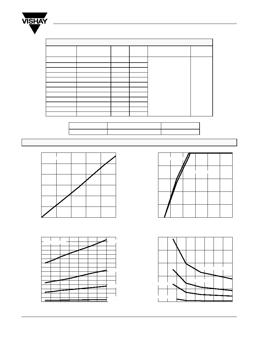
TYPICAL CHARACTERISTICS (INTERNALLY REGULATED, 25_C UNLESS NOTED)
0
50
100
150
200
250
300
0
60
120
180
240
300
Dropout Voltage vs. Load Current
I
LOAD (mA)
(mV)
V
DROP
0
25
50
75
100
125
150
175
200
225
250
275
300
325
350
375
-50
-25
0
25
50
75
100
125
150
Dropout Voltage vs. Temperature
0.0
0.5
1.0
1.5
2.0
2.5
0
1
2
3
4
5
6
V
IN
- V
OUT
Transfer Characteristic
V
IN
(V)
(V)
V
OUT
Junction Temperature (_C)
0
100
200
300
400
500
1.0
1.5
2.0
2.5
3.0
3.5
4.0
4.5
5.0
Dropout Voltage vs. V
OUT
Dropout V
oltage (mV)
V
OUT
(mV)
V
DROP
I
OUT
= 0 mA
I
OUT
= 150 mA
I
OUT
= 10 mA
I
OUT
= 75 mA
V
OUT
= 2.5 V
V
OUT
= 2.5 V
I
OUT
= 10 mA
I
OUT
= 75 mA
I
OUT
= 150 mA
I
OUT
= 300 mA
I
OUT
= 300 mA
R
LOAD
= 16.6 W
R
LOAD
= 250 W