SPICE Device Model Si4922DY
Vishay Siliconix
This document is intended as a SPICE modeling guideline and does not constitute a commercial product data sheet. Designers should refer to the appropriate
data sheet of the same number for guaranteed specification limits.
Document Number: 71563
www.vishay.com
16-Apr-01
1
N-Channel 30-V (D-S) MOSFET
CHARACTERISTICS
À N-Channel Vertical DMOS
À Macro Model (Subcircuit Model)
À Level 3 MOS
À Apply for both Linear and Switching Application
À Accurate over the -55 to 125░C Temperature Range
À Model the Gate Charge, Transient, and Diode Reverse Recovery
Characteristics
DESCRIPTION
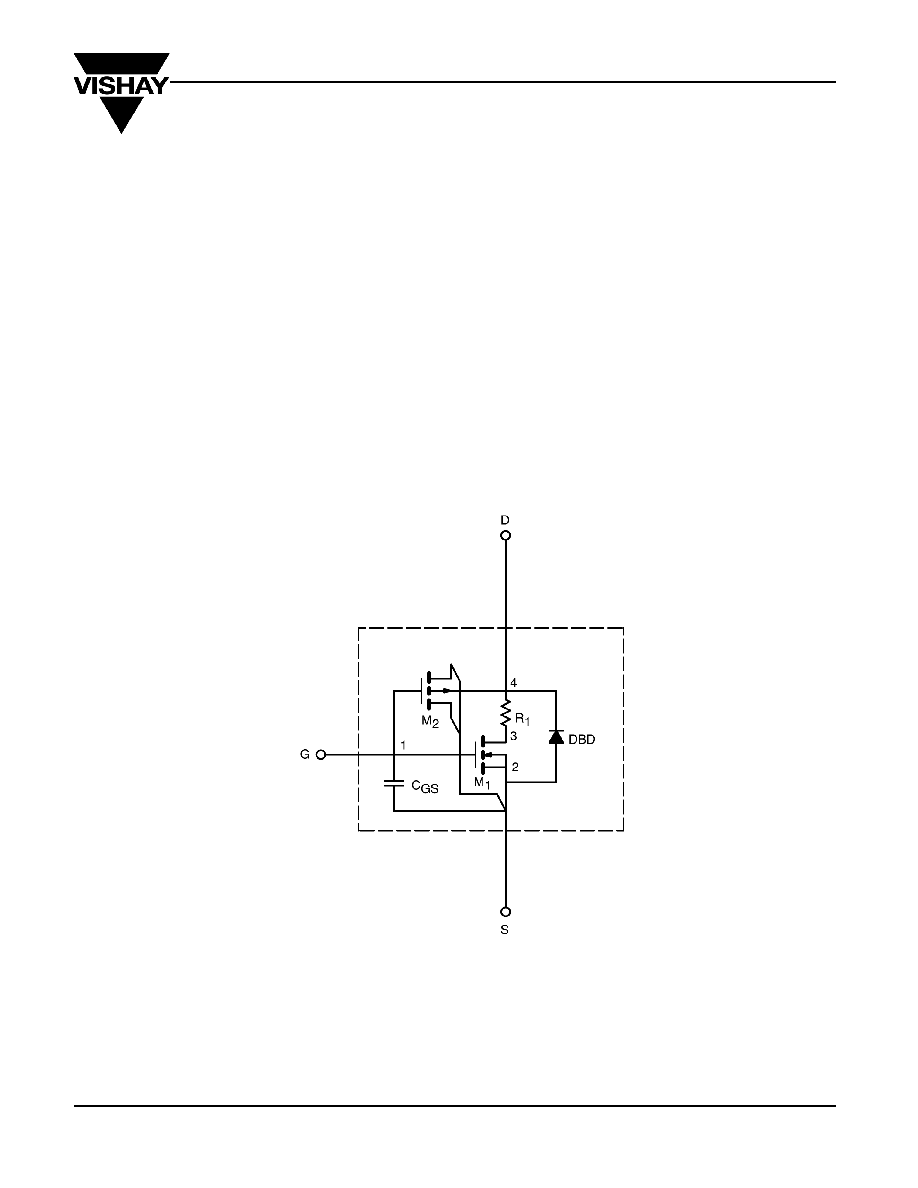
The attached spice model describes the typical electrical
characteristics of the n-channel vertical DMOS. The subcircuit
model is extracted and optimized over the
-55 to 125░C
temperature ranges under the pulsed 0-to-5V gate drive. The
saturated output impedance is best fit at the gate bias near the
threshold voltage.
A novel gate-to-drain feedback capacitance network is used to model
the gate charge characteristics while avoiding convergence difficulties
of the switched C
gd
model. All model parameter values are optimized
to provide a best fit to the measured electrical data and are not
intended as an exact physical interpretation of the device.
SUBCIRCUIT MODEL SCHEMATIC
SPICE Device Model Si4922DY
Vishay Siliconix
www.vishay.com
Document Number: 71563
2
16-Apr-01
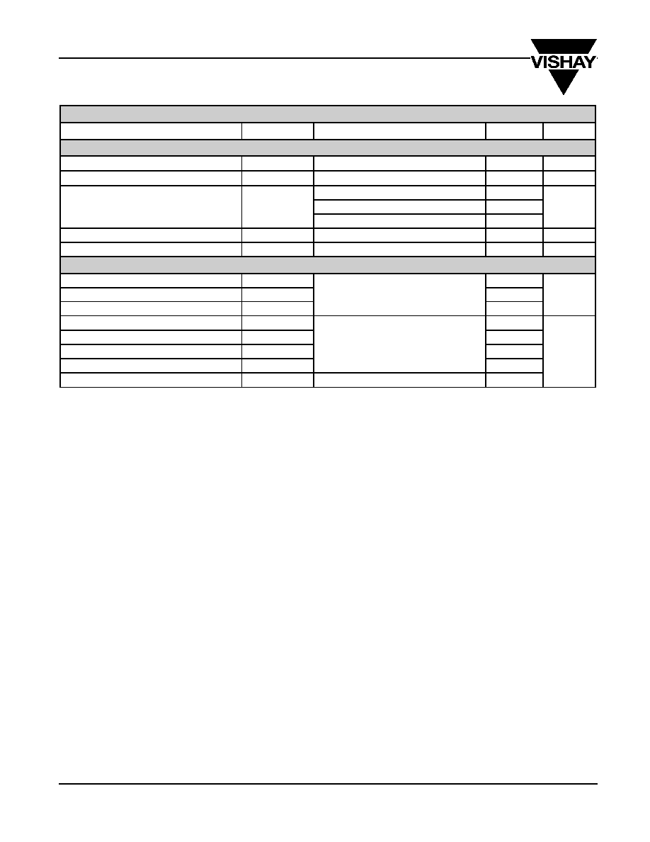
SPECIFICATIONS (T
J
= 25
░C UNLESS OTHERWISE NOTED)
Parameter
Symbol
Test Conditions
Typical
Unit
Static
Gate Threshold Voltage
V
GS(th)
V
DS
= V
GS
, I
D
= 250
ÁA
1.1
V
On-State Drain Current
a
I
D(on)
V
DS
5 V, V
GS
= 10 V
365
A
V
GS
= 10 V, I
D
= 8.8 A
0.013
V
GS
= 4.5 V, I
D
= 8.3 A
0.015
Drain-Source On-State Resistance
a
r
DS(on)
V
GS
= 2.5 V, I
D
= 7.2 A
0.024
Forward Transconductance
a
g
fs
V
DS
= 15 V, I
D
= 8.8 A
31
S
Diode Forward Voltage
a
V
SD
I
S
= 1.7 A, V
GS
= 0 V
0.72
V
Dynamic
b
Total Gate Charge
Q
g
22.8
Gate-Source Charge
Q
gs
5.8
Gate-Drain Charge
Q
gd
V
DS
= 15 V, V
GS
= 4.5 V, I
D
= 8.8 A
5.8
nC
Turn-On Delay Time
t
d(on)
13
Rise Time
t
r
17
Turn-Off Delay Time
t
d(off)
20
Fall Time
t
f
V
DD
= 15 V, R
L
= 15
I
D
1 A, V
GEN
= 10 V, R
G
= 6
47
Source-Drain Reverse Recovery Time
t
rr
I
F
= 1.7 A, di/dt = 100 A/
Ás
30
ns
Notes
a. Pulse test; pulse width
300 Ás, duty cycle 2%.
b. Guaranteed by design, not subject to production testing.
SPICE Device Model Si4922DY
Vishay Siliconix
Document Number: 71563
www.vishay.com
16-Apr-01
3
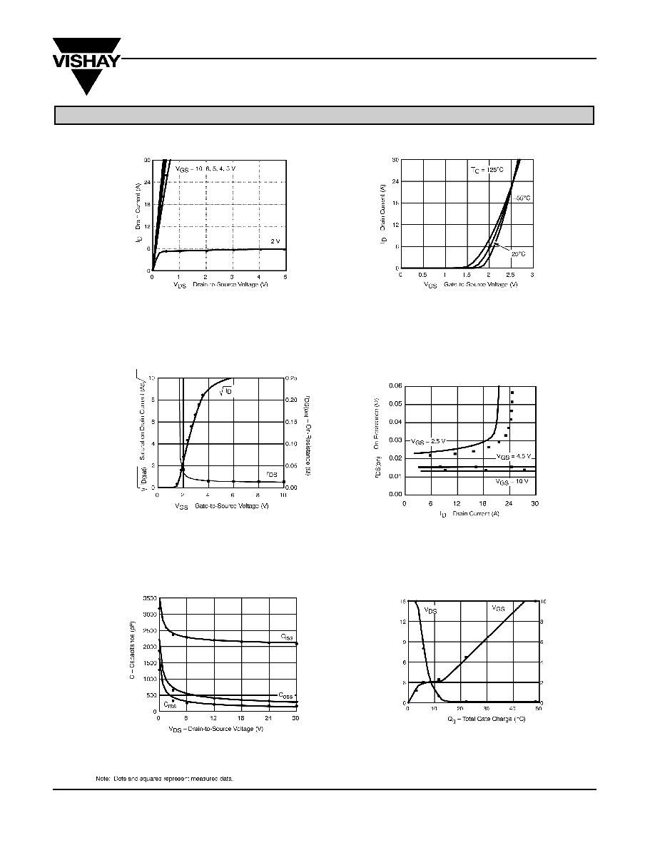
COMPARISON OF MODEL WITH MEASURED DATA (T
J
=25
░C UNLESS OTHERWISE NOTED)