FEATURES
D TrenchFETr Power MOSFET
D PWM Optimized for Fast Switching In Small
Footprint
D 100% R
g
Tested
APPLICATIONS
D Primary Side Switch for Low Power DC/DC
Converters
Si3440DV
Vishay Siliconix
New Product
Document Number: 72380
S-32412--Rev. B, 24-Nov-03
www.vishay.com
1
N-Channel 150-V (D-S) MOSFET
PRODUCT SUMMARY
V
DS
(V)
r
DS(on)
(W)
I
D
(A)
150
0.375 @ V
GS
= 10 V
1.5
150
0.400 @ V
GS
= 6.0 V
1.4
(1, 2, 5, 6) D
(3) G
(4) S
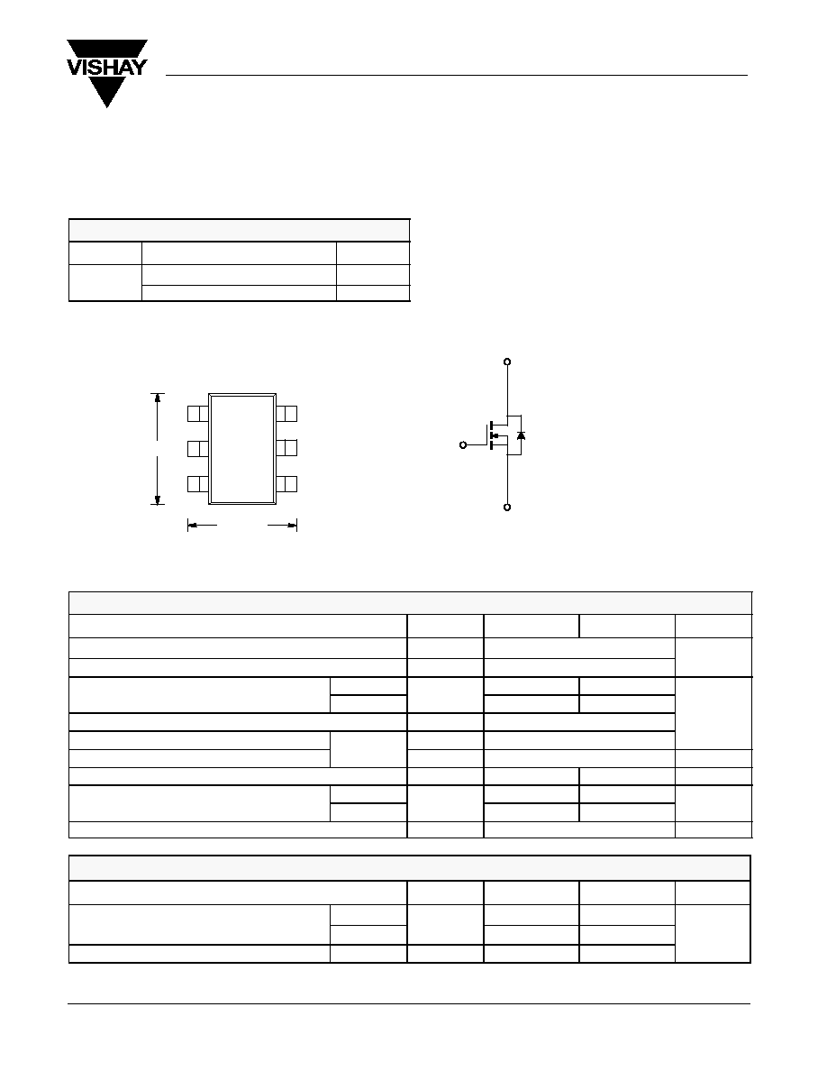
N-Channel MOSFET
TSOP-6
Top View
6
4
1
2
3
5
2.85 mm
3 mm
Ordering Information: Si3440DV-T1--E3
ABSOLUTE MAXIMUM RATINGS (T
A
= 25_C UNLESS OTHERWISE NOTED)
Parameter
Symbol
5 secs
Steady State
Unit
Drain-Source Voltage
V
DS
150
V
Gate-Source Voltage
V
GS
"20
V
Continuous Drain Current
(T
J
= 175_C)
a
T
A
= 25_C
I
D
1.5
1.2
Continuous Drain Current
(T
J
= 175_C)
a
T
A
= 85_C
I
D
1.1
0.8
A
Pulsed Drain Current
I
DM
6
A
Single Avalanche Current
L = 0 1 mH
I
AS
4
Single Avalanche Energy (Duty Cycle v1%)
L = 0.1 mH
E
AS
0.8
mJ
Continuous Source Current (Diode Conduction)
a
I
S
1.7
1.0
A
Maximum Power Dissipation
a
T
A
= 25_C
P
D
2.0
1.14
W
Maximum Power Dissipation
a
T
A
= 85_C
P
D
1.0
0.59
W
Operating Junction and Storage Temperature Range
T
J
, T
stg
-55 to 150
_C
THERMAL RESISTANCE RATINGS
Parameter
Symbol
Typical
Maximum
Unit
M i
J
ti
t A bi t
a
t v 5 sec
R
45
62.5
Maximum Junction-to-Ambient
a
Steady State
R
thJA
90
110
_C/W
Maximum Junction-to-Foot (Drain)
Steady State
R
thJF
25
30
C/W
Notes
a.
Surface Mounted on 1" x 1" FR4 Board.

Si3440DV
Vishay Siliconix
New Product
www.vishay.com
2
Document Number: 72380
S-32412--Rev. B, 24-Nov-03
SPECIFICATIONS (T
J
= 25_C UNLESS OTHERWISE NOTED)
Parameter
Symbol
Test Condition
Min
Typ
Max
Unit
Static
Gate Threshold Voltage
V
GS(th)
V
DS
= V
GS
, I
D
= 250 mA
2
4
V
Gate-Body Leakage
I
GSS
V
DS
= 0 V, V
GS
= "20 V
"100
nA
Zero Gate Voltage Drain Current
I
DSS
V
DS
= 150 V, V
GS
= 0 V
1
mA
Zero Gate Voltage Drain Current
I
DSS
V
DS
= 150 V, V
GS
= 0 V, T
J
= 85_C
5
mA
On-State Drain Current
a
I
D(on)
V
DS
w 5 V, V
GS
= 10
V
4
A
Drain-Source On-State Resistance
a
r
DS(on)
V
GS
= 10
V, I
D
= 1.5 A
0.310
0.375
W
Drain-Source On-State Resistance
a
r
DS(on)
V
GS
= 6.0 V, I
D
= 1.4 A
0.330
0.400
W
Forward Transconductance
a
g
fs
V
DS
= 15 V, I
D
= 1.5 A
4.1
S
Diode Forward Voltage
a
V
SD
I
S
= 1.7 A, V
GS
= 0 V
0.8
1.2
V
Dynamic
b
Total Gate Charge
Q
g
5.4
8
Gate-Source Charge
Q
gs
V
DS
= 75 V,
V
GS
= 10 V, I
D
= 1.5 A
1.1
nC
Gate-Drain Charge
Q
gd
1.9
Gate Resistance
R
g
f = 1 MHz
4
9
15
W
Turn-On Delay Time
t
d(on)
8
15
Rise Time
t
r
V
DD
= 75 V, R
L
= 75 W
10
15
ns
Turn-Off Delay Time
t
d(off)
V
DD
= 75 V, R
L
= 75 W
I
D
^ 1 A, V
GEN
= 10 V, R
G
= 6 W
20
30
ns
Fall Time
t
f
15
25
Source-Drain Reverse Recovery Time
t
rr
I
F
= 1.7 A, di/dt = 100 A/ms
40
60
ns
Notes
a.
Pulse test; pulse width v
300 ms, duty cycle v
2%.
b.
Guaranteed by design, not subject to production testing.
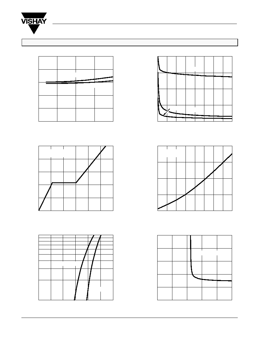
TYPICAL CHARACTERISTICS (25_C UNLESS NOTED)
0.0
0.5
1.0
1.5
2.0
2.5
3.0
3.5
4.0
0.0 0.5 1.0 1.5 2.0 2.5 3.0 3.5 4.0 4.5 5.0 5.5
0.0
0.5
1.0
1.5
2.0
2.5
3.0
3.5
4.0
0.0
0.5
1.0
1.5
2.0
2.5
3.0
3.5
4.0
V
GS
= 10 thru 5 V
T
C
= 125_C
-55_C
4 V
25_C
Output Characteristics
Transfer Characteristics
V
DS
- Drain-to-Source Voltage (V)
-
Drain Current (A)
I
D
V
GS
- Gate-to-Source Voltage (V)
-
Drain Current (A)
I
D
3 V
Si3440DV
Vishay Siliconix
New Product
Document Number: 72380
S-32412--Rev. B, 24-Nov-03
www.vishay.com
3
TYPICAL CHARACTERISTICS (25_C UNLESS NOTED)
-
On-Resistance (
r
DS(on)
W
)
0
80
160
240
320
0
10
20
30
40
50
60
70
80
0.5
1.0
1.5
2.0
2.5
-50
-25
0
25
50
75
100
125
150
0
2
4
6
8
10
0
1
2
3
4
5
6
0.0
0.1
0.2
0.3
0.4
0.5
0
1
2
3
4
V
DS
- Drain-to-Source Voltage (V)
C
rss
C
oss
C
iss
V
DS
= 75 V
I
D
= 1.5 A
I
D
- Drain Current (A)
V
GS
= 10 V
I
D
= 1.5 A
V
GS
= 10 V
V
GS
= 6.0 V
Gate Charge
On-Resistance vs. Drain Current
-
Gate-to-Source V
oltage (V)
Q
g
- Total Gate Charge (nC)
C
-
Capacitance (pF)
V
GS
Capacitance
On-Resistance vs. Junction Temperature
T
J
- Junction Temperature (_C)
(Normalized)
-
On-Resistance (
r
DS(on)
W
)
0.0
0.2
0.4
0.6
0.8
1.0
1.2
0.0
0.2
0.4
0.6
0.8
1.0
0
2
4
6
8
10
T
J
= 150_C
T
J
= 25_C
I
D
= 1.5 A
10
1
Source-Drain Diode Forward Voltage
On-Resistance vs. Gate-to-Source Voltage
-
On-Resistance (
r
DS(on)
W
)
V
SD
- Source-to-Drain Voltage (V)
V
GS
- Gate-to-Source Voltage (V)
-
Source Current (A)
I
S

Si3440DV
Vishay Siliconix
New Product
www.vishay.com
4
Document Number: 72380
S-32412--Rev. B, 24-Nov-03
TYPICAL CHARACTERISTICS (25_C UNLESS NOTED)
0
15
30
5
10
Power (W)
Single Pulse Power
Time (sec)
10
-3
10
-2
1
10
600
10
-1
10
-4
100
-1.2
-0.8
-0.4
0.0
0.4
0.8
-50
-25
0
25
50
75
100
125
150
I
D
= 250 mA
2
1
0.1
0.01
0.2
0.1
0.05
0.02
Single Pulse
Duty Cycle = 0.5
Threshold Voltage
V
ariance (V)
V
GS(th)
T
J
- Temperature (_C)
Normalized Thermal Transient Impedance, Junction-to-Ambient
Square Wave Pulse Duration (sec)
Normalized Ef
fective
T
ransient
Thermal Impedance
1. Duty Cycle, D =
2. Per Unit Base = R
thJA
= 90_C/W
3. T
JM
- T
A
= P
DM
Z
thJA(t)
t
1
t
2
t
1
t
2
Notes:
4. Surface Mounted
P
DM
1
600
10
20
0.1
0.01
100
25
Safe Operating Area
V
DS
- Drain-to-Source Voltage (V)
100
1
0.1
1
10
100
0.01
10
T
A
= 25_C
Single Pulse
-
Drain Current (A)
I
D
0.1
I
D(on)
Limited
r
DS(on)
Limited
BV
DSS
Limited
P(t) = 10
I
DM
Limited
dc
P(t) = 1
P(t) = 0.1
P(t) = 0.01
P(t) = 0.001
P(t) = 0.0001

Si3440DV
Vishay Siliconix
New Product
Document Number: 72380
S-32412--Rev. B, 24-Nov-03
www.vishay.com
5
TYPICAL CHARACTERISTICS (25_C UNLESS NOTED)
10
-3
10
-2
1
10
10
-1
10
-4
2
1
0.1
0.01
0.2
0.1
0.05
0.02
Single Pulse
Duty Cycle = 0.5
Normalized Thermal Transient Impedance, Junction-to-Foot
Square Wave Pulse Duration (sec)
Normalized Ef
fective
T
ransient
Thermal Impedance