Si2301BDS
Vishay Siliconix
Document Number: 72066
S-31990--Rev. B, 13-Oct-03
www.vishay.com
1
P-Channel 2.5-V (G-S) MOSFET
PRODUCT SUMMARY
V
DS
(V)
r
DS(on)
(W)
I
D
(A)
b
20
0.100 @ V
GS
= -4.5 V
-2.4
-20
0.150 @ V
GS
= -2.5 V
-2.0
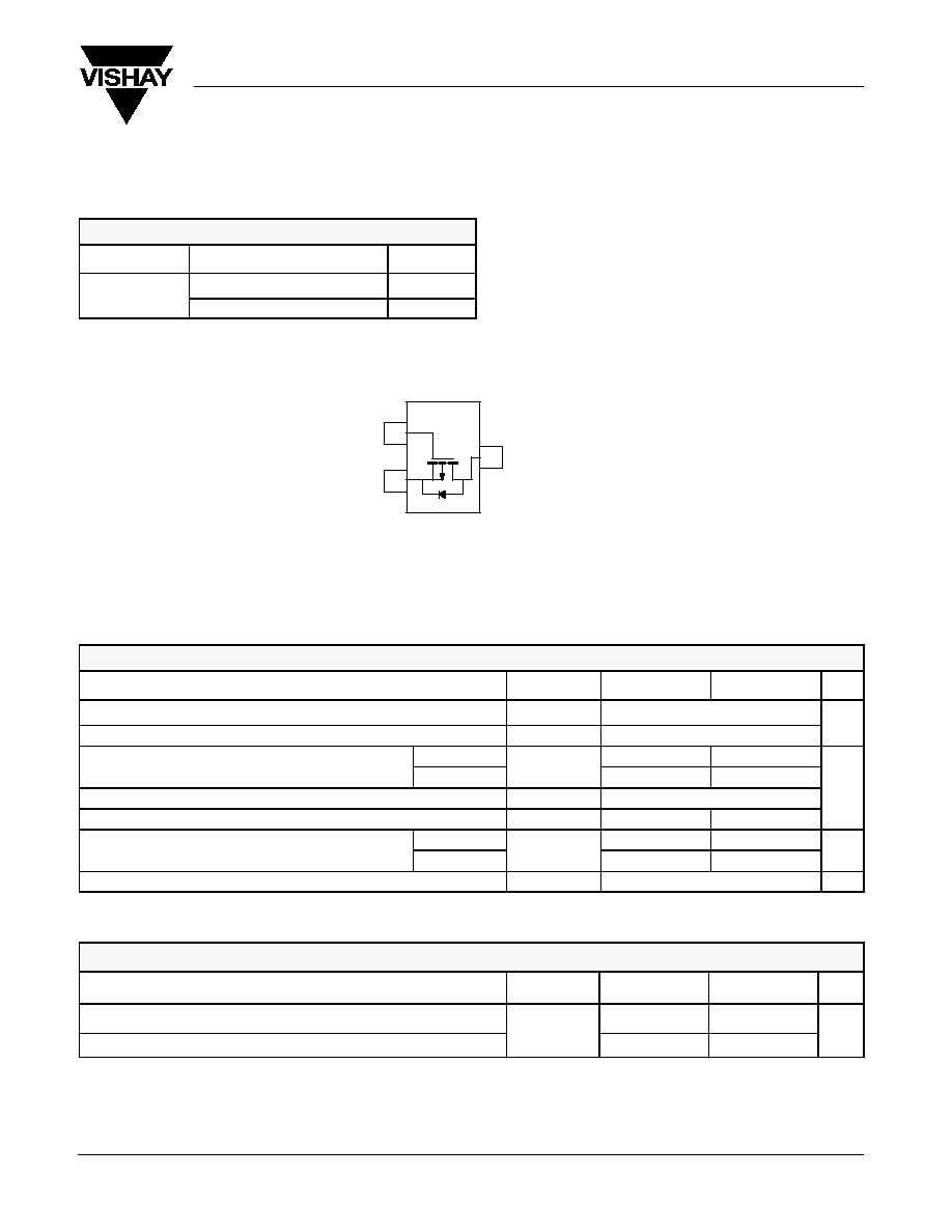
G
TO-236
(SOT-23)
S
D
Top View
2
3
1
Si2301 BDS (L1)*
*Marking Code
Ordering Information: Si2301BDS-T1
ABSOLUTE MAXIMUM RATINGS (T
A
= 25_C UNLESS OTHERWISE NOTED)
Parameter
Symbol
5 sec
Steady State
Unit
Drain-Source Voltage
V
DS
-20
V
Gate-Source Voltage
V
GS
"8
V
Continuous Drain Current
(T
J
= 150_C)
b
T
A
= 25_C
I
D
-2.4
-2.2
Continuous Drain Current
(T
J
= 150_C)
b
T
A
= 70_C
I
D
-1.9
-1.8
A
Pulsed Drain Current
a
I
DM
-10
A
Continuous Source Current (Diode Conduction)
b
I
S
-0.72
-0.6
Power Dissipation
b
T
A
= 25_C
P
D
0.9
0.7
W
Power Dissipation
b
T
A
= 70_C
P
D
0.57
0.45
W
Operating Junction and Storage Temperature Range
T
J
, T
stg
-55 to 150
_C
THERMAL RESISTANCE RATINGS
Parameter
Symbol
Typical
Maximum
Unit
Maximum Junction-to-Ambient
b
R
120
145
_C/W
Maximum Junction-to-Ambient
c
R
thJA
140
175
_C/W
Notes
a.
Pulse width limited by maximum junction temperature.
b.
Surface Mounted on FR4 Board, t v 5 sec.
c.
Surface Mounted on FR4 Board.
For SPICE model information via the Worldwide Web: http://www.vishay.com/www/product/spice.htm
Si2301BDS
Vishay Siliconix
www.vishay.com
2
Document Number: 72066
S-31990--Rev. B, 13-Oct-03
SPECIFICATIONS (T
J
= 25_C UNLESS OTHERWISE NOTED)
Limits
Parameter
Symbol
Test Conditions
Min
Typ
Max
Unit
Static
Drain-Source Breakdown Voltage
V
(BR)DSS
V
GS
= 0 V, I
D
= -250 mA
-20
V
Gate-Threshold Voltage
V
GS(th)
V
DS
= V
GS
, I
D
= -250 mA
-0.45
-0.95
V
Gate-Body Leakage
I
GSS
V
DS
= 0 V, V
GS
= "8 V
"100
nA
Zero Gate Voltage Drain Current
I
DSS
V
DS
= -20 V, V
GS
= 0 V
-1
mA
Zero Gate Voltage Drain Current
I
DSS
V
DS
= -20 V, V
GS
= 0 V, T
J
= 55_C
-10
mA
On State Drain Current
a
I
D( )
V
DS
v -5 V, V
GS
= -4.5 V
-6
A
On-State Drain Current
a
I
D(on)
V
DS
v -5 V, V
GS
= -2.5 V
-3
A
Drain Source On Resistance
a
r
DS( )
V
GS
= -4.5 V, I
D
= -2.8 A
0.080
0.100
W
Drain-Source On-Resistance
a
r
DS(on)
V
GS
= -2.5 V, I
D
= -2.0 A
0.110
0.150
W
Forward Transconductance
a
g
fs
V
DS
= -5 V, I
D
= -2.8 A
6.5
S
Diode Forward Voltage
V
SD
I
S
= -0.75 A, V
GS
= 0 V
-0.80
-1.2
V
Dynamic
b
Total Gate Charge
Q
g
4.5
10
Gate-Source Charge
Q
gs
V
DS
= -6 V, V
GS
= -4.5 V
I
D
^ -2.8 A
0.7
nC
Gate-Drain Charge
Q
gd
I
D
^ -2.8 A
1.1
Input Capacitance
C
iss
375
Output Capacitance
C
oss
V
DS
= -6 V, V
GS
= 0, f = 1 MHz
95
pF
Reverse Transfer Capacitance
C
rss
65
Switching
c
Turn On Time
t
d(on)
20
30
Turn-On Time
t
r
V
DD
= -6 V, R
L
= 6 W
I
D
^ -1 0 A V
GEN
= -4 5 V
40
60
ns
Turn-Off Time
t
d(off)
I
D
^ -1.0 A, V
GEN
= -4.5 V
R
G
= 6 W
30
45
ns
Turn-Off Time
t
f
20
30
Notes
a.
Pulse test: PW v300 ms duty cycle v2%.
b.
For DESIGN AID ONLY, not subject to production testing.
c.
Switching time is essentially independent of operating temperature. S FaxBack 408-970-5600
Si2301BDS
Vishay Siliconix
Document Number: 72066
S-31990--Rev. B, 13-Oct-03
www.vishay.com
3
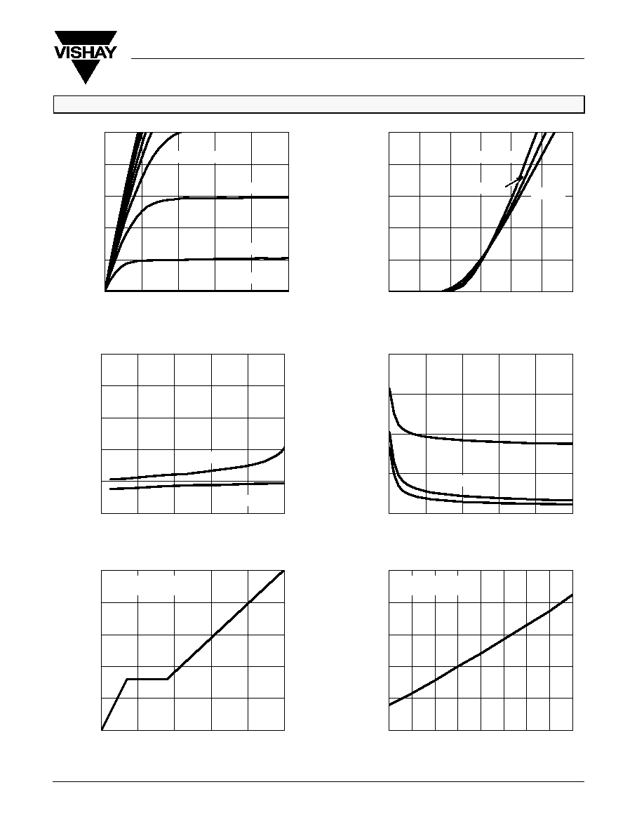
TYPICAL CHARACTERISTICS (25_C UNLESS NOTED)
0.6
0.8
1.0
1.2
1.4
1.6
-50
-25
0
25
50
75
100
125
150
0
1
2
3
4
5
0
1
2
3
4
5
0
200
400
600
800
0
4
8
12
16
20
0.0
0.1
0.2
0.3
0.4
0.5
0
2
4
6
8
10
0
2
4
6
8
10
0.0
0.5
1.0
1.5
2.0
2.5
3.0
0
2
4
6
8
10
0
1
2
3
4
5
On-Resistance vs. Drain Current
Output Characteristics
Transfer Characteristics
V
DS
- Drain-to-Source Voltage (V)
-
Drain Current (A)
I D
V
GS
- Gate-to-Source Voltage (V)
-
Drain Current (A)
I D
T
C
= -55_C
125_C
V
GS
= 5 thru 2.5 V
1.5 V
2 V
Gate Charge
-
Gate-to-Source V
oltage (V)
Q
g
- Total Gate Charge (nC)
V
DS
- Drain-to-Source Voltage (V)
C
-
Capacitance (pF)
V
GS
C
rss
C
oss
C
iss
V
DS
= 10 V
I
D
= 2.8 A
-
On-Resistance (
r DS(on)
W
)
I
D
- Drain Current (A)
Capacitance
On-Resistance vs. Junction Temperature
V
GS
= 4.5 V
I
D
= 2.8 A
T
J
- Junction Temperature (_C)
(Normalized)
-
On-Resistance (
r DS(on)
W
)
V
GS
= 2.5 V
V
GS
= 4.5 V
25_C
1 V
Si2301BDS
Vishay Siliconix
www.vishay.com
4
Document Number: 72066
S-31990--Rev. B, 13-Oct-03
TYPICAL CHARACTERISTICS (25_C UNLESS NOTED)
0.0
0.1
0.2
0.3
0.4
0.5
0.6
0
1
2
3
4
5
V
ariance (V)
V
GS(th)
-
Source Current (A)
I S
-0.2
-0.1
0.0
0.1
0.2
0.3
0.4
-50
-25
0
25
50
75
100
125
150
T
J
= 150_C
Source-Drain Diode Forward Voltage
On-Resistance vs. Gate-to-Source Voltage
Threshold Voltage
Single Pulse Power
Square Wave Pulse Duration (sec)
-
On-Resistance (
r DS(on)
W
)
V
SD
- Source-to-Drain Voltage (V)
V
GS
- Gate-to-Source Voltage (V)
T
J
- Temperature (_C)
Time (sec)
Power (W)
I
D
= 2.8 A
I
D
= 250 mA
10
0.1
0
0.2
0.4
0.6
0.8
1.0
1.2
T
J
= 25_C
1
T
A
= 25_C
Safe Operating Area
V
DS
- Drain-to-Source Voltage (V)
100
1
0.1
1
10
100
0.01
10
-
Drain Current (A)
I
D
0.1
10 ms
100 ms
1 ms
10 ms
100 ms
T
A
= 25_C
Single Pulse
10
8
6
4
2
0
0.01
0.1
1
10
100
1000
dc, 100 s, 10 s, 1 s
Si2301BDS
Vishay Siliconix
Document Number: 72066
S-31990--Rev. B, 13-Oct-03
www.vishay.com
5
TYPICAL CHARACTERISTICS (25_C UNLESS NOTED)
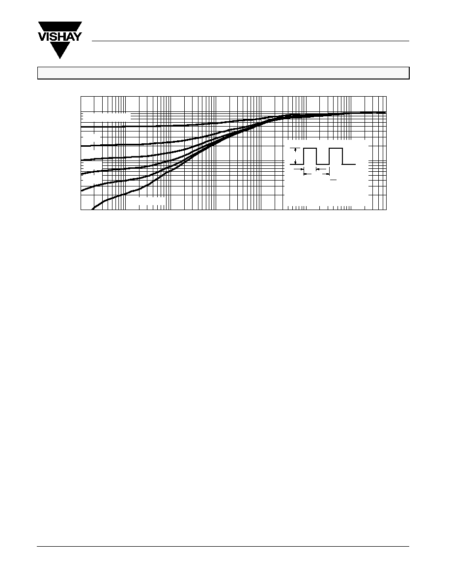
Normalized Thermal Transient Impedance, Junction-to-Ambient
Square Wave Pulse Duration (sec)
Normalized Ef
fective
T
ransient
Thermal Impedance
2
1
0.1
0.01
10
-4
10
-3
10
-2
10
-1
1
10
600
0.2
0.1
0.05
0.02
Single Pulse
Duty Cycle = 0.5
1. Duty Cycle, D =
2. Per Unit Base = R
thJA
= 62.5_C/W
3. T
JM
- T
A
= P
DM
Z
thJA(t)
t
1
t
2
t
1
t
2
Notes:
4. Surface Mounted
P
DM
100