FEATURES
D TrenchFETr Power MOSFET: 1.5-V Rated
D Ultra-Low On-Resistance
D RoHS Compliant
APPLICATIONS
D Load Switch for Portable Devices
- Guaranteed Operation at V
GS
= 1.5 V
Critical for Optimezed Design and Longer
Battery Life
Si1499DH
Vishay Siliconix
New Product
Document Number: 73338
S-50834--Rev. B, 02-May-05
www.vishay.com
1
P-Channel 1.5-V (G-S) MOSFET
PRODUCT SUMMARY
V
DS
(V)
r
DS(on)
(W)
I
D
(A)
c
Q
g
(Typ)
0.078 @ V
GS
= -4.5 V
-1.6
-8
0.095 @ V
GS
= -2.5 V
-1.6
10 5 nC
-8
0.115 @ V
GS
= -1.8 V
-1.6
10.5 nC
0.153 @ V
GS
= -1.5 V
-1.6
Ordering Information: Si1499DH-T1--E3 (Lead (Pb)-Free)
S
G
D
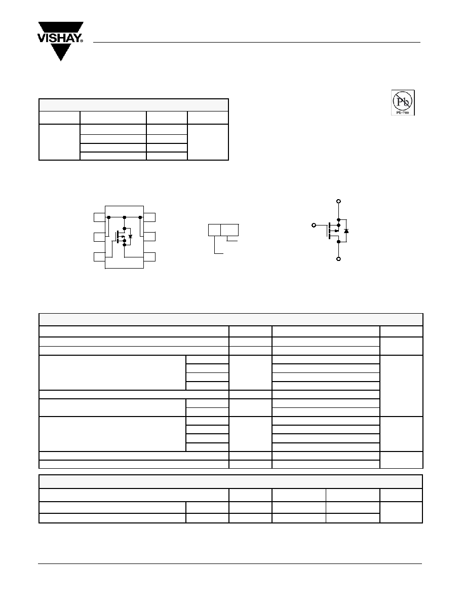
P-Channel MOSFET
SOT-363
SC-70 (6-LEADS)
6
4
1
2
3
5
Top View
D
D
G
D
D
S
Marking Code
BI
XX
Lot Traceability
and Date Code
Part #
Code
YY
ABSOLUTE MAXIMUM RATINGS (T
A
= 25_C UNLESS OTHERWISE NOTED)
Parameter
Symbol
Limit
Unit
Drain-Source Voltage
V
DS
-8
V
Gate-Source Voltage
V
GS
"5
V
T
C
= 25_C
-1.6
c
Continuous Drain Current
(T
J
= 150_C)
a, b
T
C
= 70_C
I
D
-1.6
c
Continuous Drain Current
(T
J
= 150_C)
a, b
T
A
= 25_C
I
D
-1.6
a, b, c
T
A
= 70_C
-1.6
a, b, c
A
Pulsed Drain Current (10 ms Pulse Width)
I
DM
-6.5
c
Continuous Source Drain Diode Current
a, b
T
C
= 25_C
I
S
-1.6
c
Continuous Source-Drain Diode Current
a, b
T
A
= 25_C
I
S
-1.3
a, b
T
C
= 25_C
2.78
Maximum Power Dissipation
a, b
T
C
= 70_C
P
D
1.78
W
Maximum Power Dissipation
a, b
T
A
= 25_C
P
D
2.5
a, b
W
T
A
= 70_C
1
a, b
Operating Junction and Storage Temperature Range
T
J
, T
stg
-55 to 150
_C
Soldering Recommendations (Peak Temperature)
c, d
260
_C
THERMAL RESISTANCE RATINGS
Parameter
Symbol
Typical
Maximum
Unit
Maximum Junction-to-Ambient
a, d
t p 5 sec
R
thJA
60
80
_C/W
Maximum Junction-to-Foot (Drain)
Steady State
R
thJF
34
45
_C/W
Notes:
a.
Surface Mounted on 1" x 1" FR4 Board.
b.
t = 5 sec
c.
Package limited.
d.
Maximum under steady state conditions is 125 _C/W.
Si1499DH
Vishay Siliconix
New Product
www.vishay.com
2
Document Number: 73338
S-50834--Rev. B, 02-May-05
SPECIFICATIONS (T
J
= 25_C UNLESS OTHERWISE NOTED)
Parameter
Symbol
Test Condition
Min
Typ
Max
Unit
Static
Drain-Source Breakdown Voltage
V
DS
V
GS
= 0 V, I
D
= -250 mA
-8
V
V
DS
Temperature Coefficient
DV
DS
/T
J
I
D
= -250 mA
-9
mV/_C
V
GS(th)
Temperature Coefficient
DV
GS(th)
/T
J
I
D
= -250 mA
-2.2
mV/_C
Gate Source Threshold Voltage
V
GS(th)
V
DS
= V
GS
, I
D
= -250 mA
-0.35
-0.8
V
Gate-Source Threshold Voltage
V
GS(th)
V
DS
= V
GS
, I
D
= -5 mA
-0.55
V
Gate-Source Leakage
I
GSS
V
DS
= 0 V, V
GS
= -5 V
-100
ns
Zero Gate Voltage Drain Current
I
DSS
V
DS
= -8 V, V
GS
= 0 V
-1
mA
Zero Gate Voltage Drain Current
I
DSS
V
DS
= -8 V, V
GS
= 0 V, T
J
= 55_C
-10
mA
On-State Drain Current
a
I
D(on)
V
DS
v 5 V, V
GS
= -4.5
V
-6.5
A
V
GS
= -4.5
V, I
D
= -2.0 A
0.0622
0.078
Drain-Source On-State Resistance
a
r
DS(on)
V
GS
= -2.5 V, I
D
= -1.9 A
0.078
0.095
W
Drain-Source On-State Resistance
a
r
DS(on)
V
GS
= - 1.8 V, I
D
= -0.8 A
0.094
0.115
W
V
GS
= - 1.5 V, I
D
= -0.5 A
0.118
0.153
Forward Transconductance
a
g
fs
V
DS
= -4 V, I
D
= -2.0 A
8
S
Dynamic
b
Input Capacitance
C
iss
650
Output Capacitance
C
oss
V
DS
= -4 V, V
GS
= 0 V, f = 1 MHz
220
pF
Reverse Transfer Capacitance
C
rss
122
p
Total Gate Charge
Q
g
10.5
16
Gate-Source Charge
Q
gs
V
DS
= -4 V,
V
GS
= -4.5 V, I
D
=
-1.6 A
1.3
nC
Gate-Drain Charge
Q
gd
1.9
C
Gate Resistance
R
g
f = 1 MHz
9.5
W
Turn-On Delay Time
t
d(on)
9
14
Rise Time
t
r
V
DD
=- 4 V, R
L
= 2 W
40
60
Turn-Off Delay Time
t
d(off)
V
DD
= 4 V, R
L
= 2 W
I
D
^ -2 A, V
GEN
= -4.5 V, R
g
= 1 W
50
75
Fall Time
t
f
g
60
90
ns
Turn-On Delay Time
t
d(on)
8
15
ns
Rise Time
t
r
V
DD
= -4 V, R
L
= 2 W
40
60
Turn-Off Delay Time
t
d(off)
V
DD
= 4 V, R
L
= 2 W
I
D
^ -2 A, V
GEN
= -8 V, R
g
= 1 W
46
70
Fall Time
t
f
g
60
90
Drain-Source Body Diode Characteristics
Continuous Source-Drain Diode Current
I
S
T
C
= 25_C
-1.6
A
Pulse Diode Forward Current
I
SM
-6.5
A
Body Diode Voltage
V
SD
I
S
= -2.4 A, V
GS
= 0 V
-0.7
-1.2
V
Body Diode Reverse Recovery Time
t
rr
25
38
ns
Body Diode Reverse Recovery Charge
Q
rr
I
F
= 2 0 A di/dt = 100 A/ms T
J
= 25_C
7
11
nC
Reverse Recovery Fall Time
t
a
I
F
= -2.0 A, di/dt = 100 A/ms, T
J
= 25_C
9
ns
Reverse Recovery Rise Time
t
b
16
ns
Notes
a.
Pulse test; pulse width v
300 ms, duty cycle v
2%.
b.
Guaranteed by design, not subject to production testing.
Stresses beyond those listed under "Absolute Maximum Ratings" may cause permanent damage to the device. These are stress ratings only, and functional operation
of the device at these or any other conditions beyond those indicated in the operational sections of the specifications is not implied. Exposure to absolute maximum
rating conditions for extended periods may affect device reliability.

Si1499DH
Vishay Siliconix
New Product
Document Number: 73338
S-50834--Rev. B, 02-May-05
www.vishay.com
3
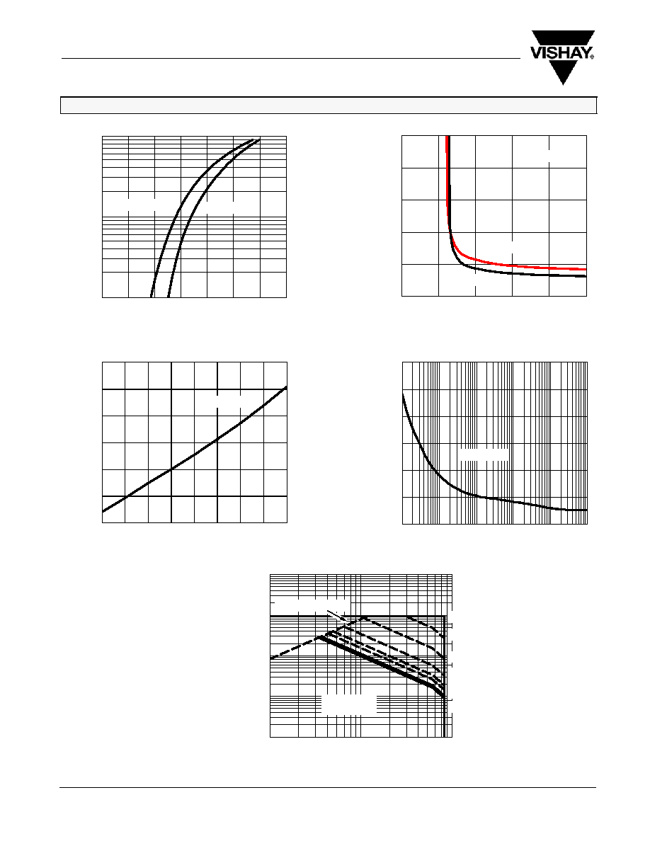
TYPICAL CHARACTERISTICS (25_C UNLESS NOTED)
0.00
0.05
0.10
0.15
0.20
0.25
0
2
4
6
8
10
0
1
2
3
4
5
0
2
4
6
8
10
12
0.6
0.8
1.0
1.2
1.4
1.6
-50
-25
0
25
50
75
100
125
150
0
200
400
600
800
1000
0
1
2
3
4
5
6
7
8
C
rss
C
oss
C
iss
I
D
= 2 A
I
D
= 2 A
V
GS
= 2.5 V
Gate Charge
On-Resistance vs. Drain Current and Gate Voltage
-
Gate-to-Source V
oltage (V)
Q
g
- Total Gate Charge (nC)
V
DS
- Drain-to-Source Voltage (V)
C
-
Capacitance (pF)
V
GS
I
D
- Drain Current (A)
Capacitance
On-Resistance vs. Junction Temperature
T
J
- Junction Temperature (_C)
V
GS
= 4.5 V
r
DS
(
on)
-
On-Resiistance
(Normalized)
0
2
4
6
8
10
0.0
0.5
1.0
1.5
2.0
2.5
0
2
4
6
8
10
0.0
0.5
1.0
1.5
2.0
V
GS
= 5 thru 2 V
25_C
T
C
= -55_C
125_C
1.5 V
Output Characteristics
Transfer Characteristics
V
DS
- Drain-to-Source Voltage (V)
-
Drain Current (A)
I
D
V
GS
- Gate-to-Source Voltage (V)
-
Drain Current (A)
I
D
r
DS
(
on)
-
On-Resistance (m
W
)
1 V
V
GS
= 1.8 V
V
GS
= 1.5 V
V
DS
= 4 V
V
DS
= 5.6 V
V
GS
= 4.5 V
V
GS
= 2.5 V
Si1499DH
Vishay Siliconix
New Product
www.vishay.com
4
Document Number: 73338
S-50834--Rev. B, 02-May-05
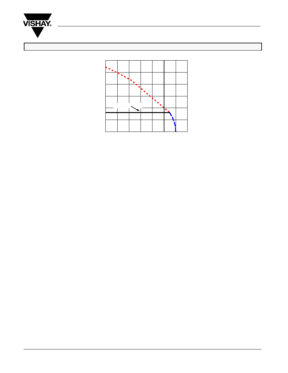
TYPICAL CHARACTERISTICS (25_C UNLESS NOTED)
0.0
0.1
0.2
0.3
0.4
0.5
0
1
2
3
4
5
1.0
1.4
0.1
1
10
0.0
0.2
0.4
0.6
0.8
T
J
= 25_C
T
J
= 150_C
Source-Drain Diode Forward Voltage
V
SD
- Source-to-Drain Voltage (V)
-
Source Current (A)
I
S
I
D
= 2 A
On-Resistance vs. Gate-to-Source Voltage
V
GS
- Gate-to-Source Voltage (V)
-0.2
-0.1
0.0
0.1
0.2
0.3
0.4
-50
-25
0
25
50
75
100
125
150
I
D
= 250 mA
Threshold Voltage
T
J
- Temperature (_C)
0
8
12
2
6
Power (W)
Time (sec)
10
1
1000
0.1
0.01
Single Pulse Power, Junction-to-Ambient
r
DS
(
on)
-
Drain-to-Source On-Resistance (
W
)
V
GS
(t
h
)
(V)
Safe Operating Area, Junction-to-Ambient
100
1
0.1
1
10
0.01
10
-
Drain Current (A)
I
D
0.1
1 ms
T
A
= 25_C
Single Pulse
10 ms
100 ms
dc. 100 s,
*Limited by r
DS(on)
V
DS
- Drain-to-Source Voltage (V)
*V
GS
u minimum V
GS
at which r
DS(on)
is
specified
1 s
T
J
= 25_C
T
J
= 125_C
1.2
10
100
4
T
A
= 25_C
10 s
10 ms, 100 ms
Si1499DH
Vishay Siliconix
New Product
Document Number: 73338
S-50834--Rev. B, 02-May-05
www.vishay.com
5
TYPICAL CHARACTERISTICS (25_C UNLESS NOTED)
0
1
2
3
4
5
6
0
25
50
75
100
125
150
175
Package Limited
Current De-Rating*
I
D
-
Drain Current (A)
T
C
- Case Temperature (_C)
*The power dissipation P
D
is based on T
J(max)
= 175_C, using junction-to-case thermal resistance, and is more useful in settling the upper dissipation limit for
cases where additional heatsinking is used. It is used to determine the current rating, when this rating falls below the package limit.