VISHAY
SFH6943
Document Number 83688
Rev. 1.3, 20-Apr-04
Vishay Semiconductors
www.vishay.com
1
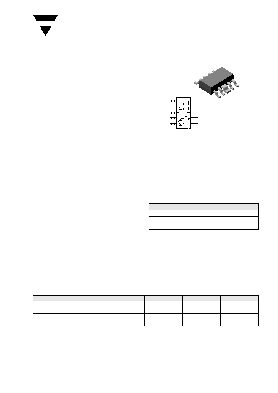
i179077
A1
A2
Com. C3
A4
A5
10 E1
9 E2
8 Com. C
7 E3
6 E4
Optocoupler, Phototransistor Output, SOT223/10, Quad
Channel
Features
· Transistor Optocoupler in SOT223/10 Package
· End Stackable, 1.27 mm Spacing
· Low Current Input
· Very High CTR, 150 % Typical at I
F
= 1 mA,
V
CE
= 5 V
· Good CTR Linearity Versus Forward Current
· Minor CTR Degradation
· High Collector-Emitter Voltage, V
CEO
=70 V
· Low Coupling Capacitance
· High Common Mode Transient Immunity
· Isolation Test Voltage: 1768 V
RMS
Agency Approvals
· UL File #E76222 System Code V
· CSA 93751
Applications
Telecommunication
SMT
PCMCIA
Instrumentation
Description
The SFH6943 is a four channel mini-optocoupler suit-
able for high density packaged PCB application. It
has a minimum of 1768 V
RMS
isolation from input to
output. The device consists of four phototransistors
as detectors. Each channel is individually controlled.
The optocoupler is housed in a SOT223/10 package.
All the cathodes of the input LEDs and all the collec-
tors of the output transistors are common enabling a
pin count reduction from 16 pins to 10 pins-a signifi-
cant space savings as compared to four channels that
are electrically isolated individually.
Order Information
For additional information on the available options refer to
Option Information.
Absolute Maximum Ratings
T
amb
= 25 °C, unless otherwise specified
Stresses in excess of the absolute Maximum Ratings can cause permanent damage to the device. Functional operation of the device is
not implied at these or any other conditions in excess of those given in the operational sections of this document. Exposure to absolute
Maximum Rating for extended periods of the time can adversely affect reliability.
Input
Part
Remarks
SFH6943-2
CTR 63 - 200 %, SMD-10
SFH6943-3
CTR 100 - 320 %, SMD-10
SFH6943-4
CTR 160 - 500 %, SMD-10
Parameter
Test condition
Symbol
Value
Unit
Reverse voltage
V
R
3
V
DC forward current
I
F
5
mA
Surge forward current
t
P
10 µs
I
FSM
100
mA
Total power dissipation
P
diss
10
mW
www.vishay.com
2
Document Number 83688
Rev. 1.3, 20-Apr-04
VISHAY
SFH6943
Vishay Semiconductors
Output
Coupler
Electrical Characteristics
T
amb
= 25 °C, unless otherwise specified
Minimum and maximum values are testing requirements. Typical values are characteristics of the device and are the result of engineering
evaluation. Typical values are for information only and are not part of the testing requirements.
Input
Output
Parameter
Test condition
Symbol
Value
Unit
Collector-emitter voltage
V
CE
70
V
Emitter-collector voltage
V
EC
7
V
Collector current
I
C
10
mA
Surge collector current
t
P
< 1 ms
I
FSM
20
mA
Total power dissipation
P
diss
20
mW
Parameter
Test condition
Symbol
Value
Unit
Isolation test voltage (between
emitter and detector, refer to
climate DIN 40046, part 2,
Nov. 74)
t = 1 sec.
V
ISO
1768
V
RMS
Creepage
4
mm
Clearance
4
mm
Comparative tracking index per
DIN IEC 112/VDE0303, part 1
175
Isolation resistance
V
IO
= 100 V, T
amb
= 25 °C
R
IO
10
11
V
IO
= 100 V, T
amb
= 100 °C
R
IO
10
12
Storage temperature range
T
stg
- 55 to + 150
°C
Ambient temperature range
T
amb
- 55 to + 100
°C
Junction temperature
T
j
100
°C
Soldering temperature, Dip
soldering plus reflow soldering
processes
t = 10 sec. max
T
sld
260
°C
Parameter
Test condition
Symbol
Min
Typ.
Max
Unit
Forward voltage
I
F
= 5 mA
V
F
1.25
V
Reverse current
V
R
= 3 V
I
R
0.01
10
µA
Capacitance
V
R
= 0 V, f = 1 MHz
C
O
5
pF
Thermal resistance
R
thja
1000
K/W
Parameter
Test condition
Symbol
Min
Typ.
Max
Unit
Collector-emitter voltage
I
CE
= 10
µA
V
CEO
70
V
Emitter-collector voltage
I
EC
= 10
µA
V
ECO
7
V
Collector-emitter capacitance
V
CE
= 5 V, f = 1 MHz
C
CE
6
pF
Thermal resistance
R
thja
500
K/W
Collector-emitter leakage
current
V
CE
= 10 V
I
CEO
50
nA

VISHAY
SFH6943
Document Number 83688
Rev. 1.3, 20-Apr-04
Vishay Semiconductors
www.vishay.com
3
Coupler
Current Transfer Ratio
Switching Characteristics
Typical Characteristics
(T
amb
= 25
°C unless otherwise specified)
Parameter
Test condition
Symbol
Min
Typ.
Max
Unit
Coupling capacitance
C
C
1
pF
Parameter
Test condition
Part
Symbol
Min
Typ.
Max
Unit
Coupling Transfer Ratio
I
F
= 1 mA, V
CE
= 1.5 V
SFH6943-2
I
E
/I
F
63
200
%
SFH6943-3
I
E
/I
F
100
320
%
SFH6943-4
I
E
/I
F
160
500
%
I
F
= 0.5 mA, V
CC
= 5 V
SFH6943-2
I
E
/I
F
32
100
%
SFH6943-3
I
E
/I
F
50
160
%
SFH6943-4
I
E
/I
F
80
250
%
Parameter
Test condition
Symbol
Min
Typ.
Max
Unit
Turn-on time
I
E
= 2 mA, R
E
= 100
, V
CC
= 5 V
t
on
3
µs
Rise time
I
E
= 2 mA, R
E
= 100
, V
CC
= 5 V
t
r
2.6
µs
Turn-off time
I
E
= 2 mA, R
E
= 100
, V
CC
= 5 V
t
off
3.1
µs
Fall time
I
E
= 2 mA, R
E
= 100
, V
CC
= 5 V
t
f
2.8
µs
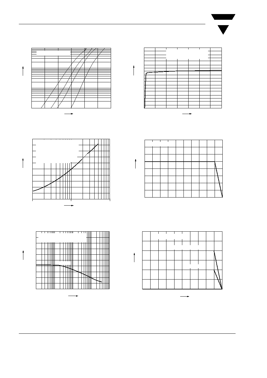
Fig. 1 Switching times (typ.)
isfh6943_01
VO
VCC = 5 V
RE = 100
F = 10 KHz
DF = 50%
IF
IE = 2 mA
Fig. 2 Switching Waveform
isfh6943_02
V0
IF
tR
tF
tOFF
tON
www.vishay.com
4
Document Number 83688
Rev. 1.3, 20-Apr-04
VISHAY
SFH6943
Vishay Semiconductors
Fig. 3 LED Current vs. LED Voltage
Fig. 4 Non-Saturated Current Transfer
Fig. 5 Transistor Capacitances (typ.)
isfh6943_03
.8
.9
1
1.1
1.2
1.3
1.4
101
100
101
102
VF/V
25°
50°
25°
85°
I F
/mA
VF = f (IF)
isfh6943_04
NCTR
I F/A
2.0
1.8
1.6
1.4
1.2
1.0
.8
.6
.4
.2
0
1 0
4
1 0
3
1 0
2
Normalized to
IF = 1 mA,
NCTR = f (IF)
VCE = 1.5 V
IF = 1 mA
isfh6943_05
CCE
25.0
22.5
20.0
17.5
15.0
12.5
10.0
7.5
5.0
2.5
0
C
CE
/ P
F
102
101
100
101
102
VCE/V
f = 1 MHz,
CCE = f (VCE)
Fig. 6 Collector-Emitter Leakage Current (typ.)
Fig. 7 Permissible Forward Current Diode
Fig. 8 Permissible Power Dissipation
isfh6943_06
103
102
101
100
101
102
103
0
10
20
30
40
50
60
70
VCE / V
I CEO
/n
A
IF = 0,
ICEO = f (VCE)
isfh6943_07
8
7
6
5
4
3
2
1
0
I F
/m
A
TA / °C
0
10
20
30
40
50
60
70
80
90 100
IF = f
isfh6943_08
30
25
20
15
10
5
0
P
tot
/m
W
TA / °C
0
10
20
30
40
50
60
70
80
90
100
Transistor
Diode
Ptot = f (TA)
VISHAY
SFH6943
Document Number 83688
Rev. 1.3, 20-Apr-04
Vishay Semiconductors
www.vishay.com
5
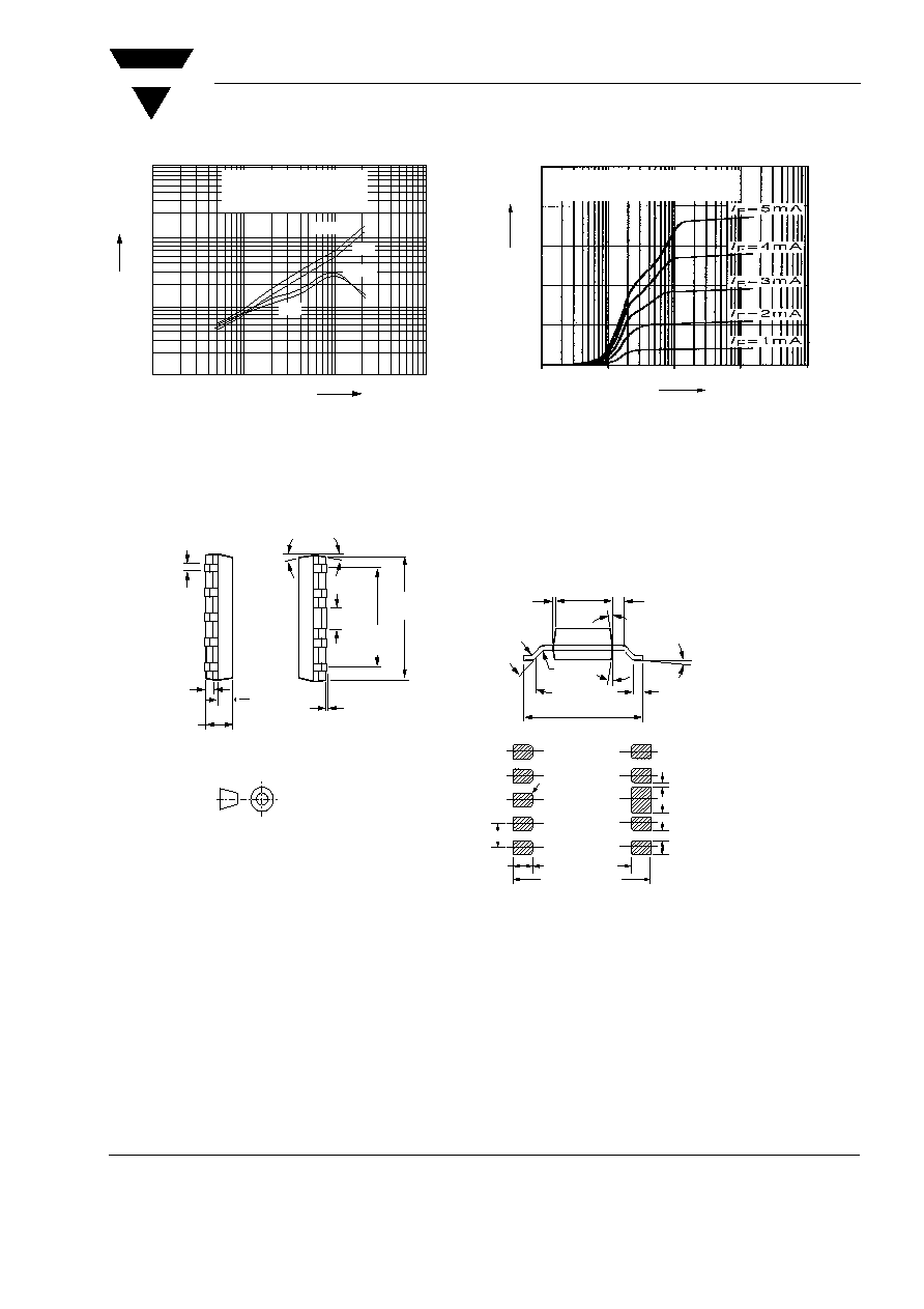
Package Dimensions in Inches (mm)
Fig. 9
isfh6943_09
103
10
101
100
t/u
s
10
2
103
104
10 5
RL / OHM
toff
tf
t on
t r
IF = 1 mA,
VCC = 5 V,
ton, tr, toff, tt = f (RL)
Fig. 10 Transistor Output Characteristics
ICE = 1 (VCE, IF)
isfh6943_10
25
20
15
10
5
0
I
CE
/mA
10
10
10
10
10
-2
-1
0
1
2
V CE/V
R .005(.13)
.050 (1.27)
.026 (.66)
.024 (.61)
.216 (5.49)
.296 (7.52)
.053 (1.35)
.040 (1.02)
.010 (.25)
i178044
.063 ± .004
(1.60 ± .10)
.018 (.46)
.035
(.90)
.016 (.41)
ISO Method A
.043
(1.09)
10°
7°
.002 +.002
.001
(.05 +.05
.03)
.256 ± .004
(6.50 ± .10)
.200 ± .005
(5.80 ± .13)
10°
0.004 (.10)
max.
0.020 (.51) min.
7°
45°
0.010R
(.25)
0°7°
.01 (.25) R
0.020 ± .004
(.51 ± .10)
0.138 ± .004
(3.51 ± .10)
.276 ± .008
(7.01 ± .20)

www.vishay.com
6
Document Number 83688
Rev. 1.3, 20-Apr-04
VISHAY
SFH6943
Vishay Semiconductors
Ozone Depleting Substances Policy Statement
It is the policy of Vishay Semiconductor GmbH to
1. Meet all present and future national and international statutory requirements.
2. Regularly and continuously improve the performance of our products, processes, distribution and
operatingsystems with respect to their impact on the health and safety of our employees and the public, as
well as their impact on the environment.
It is particular concern to control or eliminate releases of those substances into the atmosphere which are
known as ozone depleting substances (ODSs).
The Montreal Protocol (1987) and its London Amendments (1990) intend to severely restrict the use of ODSs
and forbid their use within the next ten years. Various national and international initiatives are pressing for an
earlier ban on these substances.
Vishay Semiconductor GmbH has been able to use its policy of continuous improvements to eliminate the
use of ODSs listed in the following documents.
1. Annex A, B and list of transitional substances of the Montreal Protocol and the London Amendments
respectively
2. Class I and II ozone depleting substances in the Clean Air Act Amendments of 1990 by the Environmental
Protection Agency (EPA) in the USA
3. Council Decision 88/540/EEC and 91/690/EEC Annex A, B and C (transitional substances) respectively.
Vishay Semiconductor GmbH can certify that our semiconductors are not manufactured with ozone depleting
substances and do not contain such substances.
We reserve the right to make changes to improve technical design
and may do so without further notice.
Parameters can vary in different applications. All operating parameters must be validated for each
customer application by the customer. Should the buyer use Vishay Semiconductors products for any
unintended or unauthorized application, the buyer shall indemnify Vishay Semiconductors against all
claims, costs, damages, and expenses, arising out of, directly or indirectly, any claim of personal
damage, injury or death associated with such unintended or unauthorized use.
Vishay Semiconductor GmbH, P.O.B. 3535, D-74025 Heilbronn, Germany
Telephone: 49 (0)7131 67 2831, Fax number: 49 (0)7131 67 2423