Document Number: 83648
www.vishay.com
Revision 17-August-01
2183
FEATURES
· Two Channel Optocoupler
· High Current Transfer Ratio at
I
F
=1.0 mA,
500% Min.
· Isolation Test Voltage, 3000 V
RMS
· Electrical Specifications Similar to Standard
6-pin Coupler
· Compatible with Dual Wave, Vapor Phase and
IR Reflow Soldering
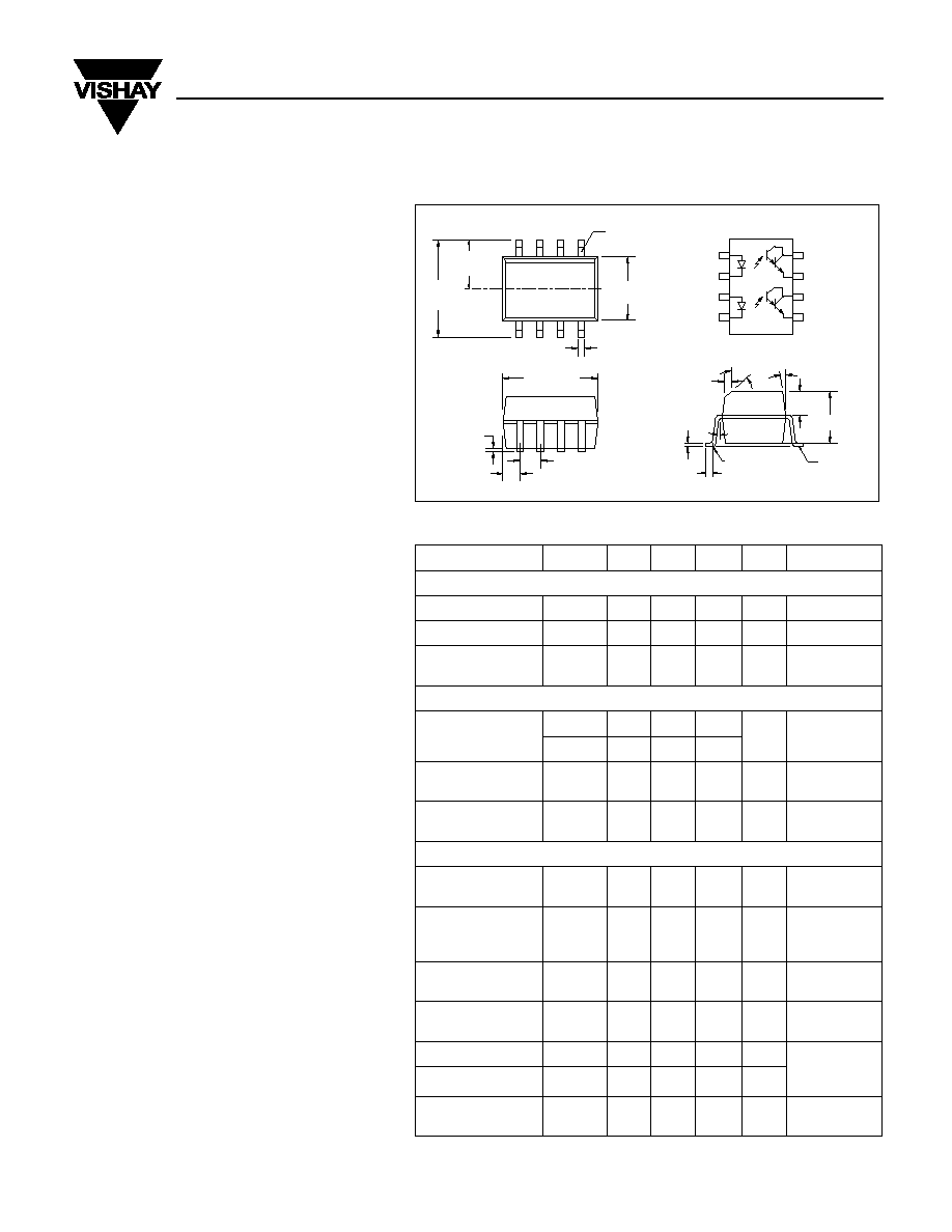
· SOIC-8 Surface Mountable Package
· Standard Lead Spacing, .05"
· Available only on Tape and Reel Option (Con-
forms to EIA Standard 481-2)
· Underwriters Lab File #E52744
DESCRIPTION
The ILD223T is a high current transfer ratio (CTR)
optocoupler. It has a Gallium Arsenide infrared LED
emitter and a silicon NPN photodarlington transis-
tor detector.
This device has CTRs tested at an LED current of
1.0 mA. This low drive current permits easy inter-
facing from CMOS to LSTTL or TTL.
The ILD223T is constructed in a standard SOIC-8A
foot print which makes it ideally suited for high den-
sity applications. In addition to eliminating through-
holes requirements, this package conforms to stan-
dards for surface mounted devices.
Maximum Ratings
(Each Channel)
Emitter
Peak Reverse Voltage ..................................... 6.0 V
Peak Pulsed Current (1.0
µ
s, 300 pps) ........... 3.0 A
Continuous Forward Current per Channel .... 30 mA
Power Dissipation at 25
°
C............................ 45 mW
Derate Linearly from 25
°
C ...................... 0.4 mW/
°
C
Detector
Collector-Emitter Breakdown Voltage............... 30 V
Emitter-Collector Breakdown Voltage.............. 5.0 V
Power Dissipation per Channel .................... 75 mW
Derate Linearly from 25
°
C ...................... 3.1 mW/
°
C
Package
Total Package Dissipation at 25
°
C Ambient
(2 LEDs + 2 Detectors, 2 Channels)....... 240 mW
Derate Linearly from 25
°
C ...................... 2.0 mW/
°
C
Storage Temperature ................... 55
°
C to +150
°
C
Operating Temperature ................ 55
°
C to +100
°
C
Soldering Time at 260
°
C ...............................10 sec
.
Table 1. Characteristics
T
A
=25
°
C
Parameter
Symbol
Min.
Typ.
Max.
Unit
Condition
Emitter
Forward Voltage
V
F
--
--
1.3
V
I
F
=1.0 mA
Reverse Current
I
R
--
0.1
100
µ
A
V
R
=6.0 V
Capacitance
C
O
--
25
--
pF
V
F
=0 V
F=1.0 MHz
Detector
Breakdown
Voltage
BV
CEO
30
--
--
V
I
C
=10
µ
A
I
E
=10
µ
A
BV
ECO
5.0
--
--
Current,
Collector-Emitter
I
CEO
--
--
50
nA
V
CE
=5.0 V
I
F
=0
Capacitance,
Collector-Emitter
C
CE
--
3.4
--
pF
V
CE
=5.0 V
Package
DC Current
Transfer Ratio
CTR
DC
500
--
--
%
I
F
=1.0 mA,
V
CE
=5.0 V
Saturation
Voltage,
Collector-Emitter
V
CE
sat
--
--
1.0
V
I
F
=1.0 mA,
I
CE
=0.5 mA
Capacitance,
Input to Output
C
IO
0.5
--
pF
--
--
Resistance,
Input to Output
R
IO
100
--
G
--
--
Turn-On Time
t
ON
15
--
µ
s
--
V
CC
=10 V
R
L
=100
I
F
=5.0 mA
Turn-Off Time
t
OFF
30
--
µ
s
--
Isolation Test
Voltage
V
IO
3000
--
--
V
RMS
t=1.0 sec.
Lead
Coplanarity
±.001 (.04)
max.
C
L
.016 (.41)
.004 (.10)
.008 (.20)
.050 (1.27) typ.
.040 (1.02)
.008 (.20)
R.010
(.25) max.
.020
±.004
(.5
±.10)
2 plcs.
.230
±.002
(5.84
±.05)
.058
(1.49)
7
°
40
°
.015
±.002
(.38
±.05)
Pin 1
.154
±.002
(3.91
±.05)
.240
(6.10)
.120
±.002
(3.05
±.05)
5
° max.
.125 (3.18)
Anode 1
Cathode 2
Anode 3
Cathode 4
8 Collector
7 Emitter
6 Collector
5 Emitter
Dimensions in inches (mm)
ILD223T
Dual Photodarlington
Small Outline Surface Mount Optocoupler
Document Number: 83648
www.vishay.com
Revision 17-August-01
2184
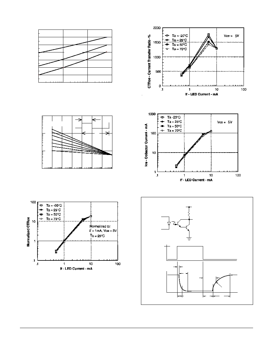
Figure 1. Forward voltage versus forward current
Figure 2. Peak LED current versus duty factor, Tau
Figure 3. Normalized CTR
CE
versus LED current
.1
1
10
100
1.4
1.3
1.2
1.1
1.0
0.9
0.8
0.7
I
F
- Forward Current - mA
V
F
- Forwar
d
V
olta
g
e
-
V
T
A
= -55
°C
T
A
= 100
°C
T
A
= 25
°C
10
-6
10
-5
10
-4
10
-3
10
-2
10
-1
10
0
10
1
10000
1000
100
10
t - LED Pulse Duration - s
If(pk) - P
eak LED Current - mA
.005
DF = /t
.05
.02
.01
.1
.2
.5
Duty Factor
t
Figure 4. CTR versus LED current
Figure 5. Collector current versus LED current
Figure 6. Switching schematic and switching timing
V
O
R
L
V
CC
=10 V
F=10 KHz,
DF=50%
IF=10 mA
I
F
t
R
V
O
t
D
t
S
t
F
t
PHL
t
PLH
V
TH
=1.5 V