
VISHAY
IL66B
Document Number 83639
Rev. 1.5, 26-Oct-04
Vishay Semiconductors
www.vishay.com
1
i179019
1
2
3
6
5
4
A
C
NC
NC
C
E
Pb
Pb-free
e3
Optocoupler, Photodarlington Output, With Internal R
BE
Features
· Internal RBE for high stability
· Isolation test voltage, 5300 V
RMS
· No base connection
· High isolation resistance
· Standard plastic DIP package
· Lead-free component
· Component in accordance to RoHS 2002/95/EC
and WEEE 2002/96/EC
Agency Approvals
· UL1577, File No. E52744 System Code H or J,
Double Protection
· BSI IEC60950 IEC60065
· CSA 93751
· DIN EN 60747-5-2 (VDE0884)
DIN EN 60747-5-5 pending
Available with Option 1
· FIMKO
Description
The IL66B is an optically coupled isolator employing
a gallium arsenide infrared emitter and a silicon pho-
todarlington detector. Switching can be accomplished
while maintaining a high degree of isolation between
driving and load circuits. They can be used to replace
reed and mercury relays with advantages of long life,
high speed switching and elimination of magnetic
fields.
Order Information
For additional information on the available options refer to
Option Information.
Absolute Maximum Ratings
T
amb
= 25 °C, unless otherwise specified
Stresses in excess of the absolute Maximum Ratings can cause permanent damage to the device. Functional operation of the device is
not implied at these or any other conditions in excess of those given in the operational sections of this document. Exposure to absolute
Maximum Rating for extended periods of the time can adversely affect reliability.
Input
Part
Remarks
IL66B-1
CTR > 200 %, DIP-6
IL66B-2
CTR > 750 %, DIP-6
IL66B-1X006
CTR > 200 %, DIP-6 400 mil (option 6)
IL66B-2X006
CTR > 750 %, DIP-6 400 mil (option 6)
IL66B-2X009
CTR > 750 %, SMD-6 (option 9)
Parameter
Test condition
Symbol
Value
Unit
Peak reverse voltage
V
R
6.0
V
Forward continuous current
I
F
60
mA
Power dissipation
P
diss
100
mW
Derate linearly from 55 °C
1.33
mW/°C
www.vishay.com
2
Document Number 83639
Rev. 1.5, 26-Oct-04
IL66B
Vishay Semiconductors
Output
Coupler
Electrical Characteristics
T
amb
= 25 °C, unless otherwise specified
Minimum and maximum values are testing requirements. Typical values are characteristics of the device and are the result of engineering
evaluation. Typical values are for information only and are not part of the testing requirements.
Input
Output
Coupler
Current Transfer Ratio
Parameter
Test condition
Symbol
Value
Unit
Collector-emitter breakdown voltage
BV
CEO
60
V
Emitter-collector breakdown voltage
BV
ECO
5.0
V
Power dissipation
P
diss
200
mW
Derate linearly from 25 °C
2.6
mW/°C
Parameter
Test condition
Symbol
Value
Unit
Isolation test voltage
t = 1.0 sec.
V
ISO
5300
V
RMS
Isolation resistance
V
IO
= 500 V, T
amb
= 25 °C
R
IO
10
12
V
IO
= 500 V, T
amb
= 100 °C
R
IO
10
11
Total dissipation
P
tot
250
mW
Derate linearly
from 25 °C
3.3
mW/°C
Creepage path
7
min mm
Clearance path
7
min mm
Storage temperature
T
stg
- 55 to + 150
°C
Operating temperature
T
amb
- 55 to + 100
°C
Lead soldering time
at 260 °C
T
sld
10
sec.
Parameter
Test condition
Symbol
Min
Typ.
Max
Unit
Forward voltage
I
F
= 10 mA
V
F
1.25
1.5
V
Reverse current
V
R
= 3.0 V
I
R
0.01
100
µA
Capacitance
V
R
= 0
C
O
25
pF
Parameter
Test condition
Symbol
Min
Typ.
Max
Unit
Collector-emitter breakdown
voltage
I
C
= 100
µA
BV
CEO
60
V
Collector-emitter leakage
current
V
CE
= 50 V, I
F
= 0
I
CEO
1.0
100
nA
Parameter
Test condition
Symbol
Min
Typ.
Max
Unit
Saturation voltage
I
C
= 10 mA
V
CEsat
1.0
V
Parameter
Test condition
Part
Symbol
Min
Typ.
Max
Unit
Current Transfer Ratio
I
F
= 2.0 mA, V
CE
= 5.0 V
IL66B-1
CTR
200
%
IL66B-2
CTR
750
1000
%
IL66B
Document Number 83639
Rev. 1.5, 26-Oct-04
Vishay Semiconductors
www.vishay.com
3
Switching Characteristics
Typical Characteristics (Tamb = 25
°C unless otherwise specified)
Parameter
Test condition
Symbol
Min
Typ.
Max
Unit
Turn-On, Turn-Off time
V
CC
= 10 V, I
F
= 2 mA,
R
L
= 100
t
on
, t
off
200
µs
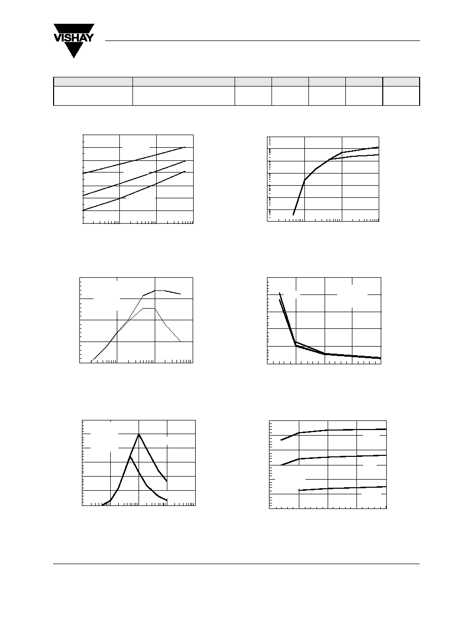
Figure 1. Forward Voltage vs. Forward Current
Figure 2. Normalized Non-saturated and Saturated CTR
CE
vs.
LED Current
Figure 3. Normalized Non-saturated and Saturated CTR
CE
vs.
LED Current
iil66b_01
IF - Forward Current - mA
100
10
1
.1
0.7
0.8
0.9
1.0
1.1
1.2
1. 3
1.4
VF
-
F
orward
Voltage
-
V
Ta = 55°C
Ta = 25°C
Ta = 85°C
iil66b_02
10 0
10
1
.1
0.0
0.5
1.0
1.5
2.0
Vce = 1 V
Vce = 5 V
IF - LED Current - mA
NCTRce
-
Normalized
CTRce
Normalized to:
Vce = 5 V
IF = 2 mA
iil66b_03
0.0
0.2
0.4
0.6
0.8
1.0
1.2
.1
10
100
1000
Vce = 5 V
Vce = .4 V
IF - LED Current - mA
NCTRce
-
Normalized
CTRce
Vce = 5 V
IF = 10 mA
Normalized to:
1
Figure 4. Non-Saturated and Saturated Collector Emitter Current
vs. LED Current
Figure 5. High to low Propagation Delay vs. Collector Load
Resistance and LED Current
Figure 6. Low to High Propagation Delay vs. Collector Load
Resistance and LED Current
iil66b_04
.1
10
100
.001
.01
.1
1
10
100
1000
10000
Vce = 5 V
Vce = .4 V
IF - LED Current - mA
Ice
-
Collector-emitter
current
-
m
A
1
iil66b_05
10
15
20
0
10
20
30
40
50
220
i
10 K
i
IF - LED Current - mA
Vcc = 5 V
Vth = 1.5 V
tpHL
-
H
igh/Low
Propagation
Delay
-
µ
s
0
5
iil66b_06
10
15
20
0
25
50
75
100
125
150
220 K
2 K
10 K
IF - LED Current - mA
tpLH
-
Low/High
Propagation
Delay
-
µ
s
Vcc = 5 V
Vth = 1.5 V
5
0

www.vishay.com
4
Document Number 83639
Rev. 1.5, 26-Oct-04
IL66B
Vishay Semiconductors
Package Dimensions in Inches (mm)
i178004
.010 (.25)
typ.
.114 (2.90)
.130 (3.0)
.130 (3.30)
.150 (3.81)
.031 (0.80) min.
.300 (7.62)
typ.
.031 (0.80)
.035 (0.90)
.100 (2.54) typ.
.039
(1.00)
Min.
.018 (0.45)
.022 (0.55)
.048 (0.45)
.022 (0.55)
.248 (6.30)
.256 (6.50)
.335 (8.50)
.343 (8.70)
pin one ID
6
5
4
1
2
3
18°
3°9°
.300.347
(7.628.81)
4°
typ.
ISO Method A
.014 (0.35)
.010 (0.25)
.400 (10.16)
.430 (10.92)
.307 (7.8)
.291 (7.4)
.407 (10.36)
.391 (9.96)
Option 6
18493
min.
.315 (8.00)
.020 (.51)
.040 (1.02)
.300 (7.62)
ref.
.375 (9.53)
.395 (10.03)
.012 (.30) typ.
.0040 (.102)
.0098 (.249)
15° max.
Option 9

IL66B
Document Number 83639
Rev. 1.5, 26-Oct-04
Vishay Semiconductors
www.vishay.com
5
Ozone Depleting Substances Policy Statement
It is the policy of Vishay Semiconductor GmbH to
1. Meet all present and future national and international statutory requirements.
2. Regularly and continuously improve the performance of our products, processes, distribution and
operatingsystems with respect to their impact on the health and safety of our employees and the public, as
well as their impact on the environment.
It is particular concern to control or eliminate releases of those substances into the atmosphere which are
known as ozone depleting substances (ODSs).
The Montreal Protocol (1987) and its London Amendments (1990) intend to severely restrict the use of ODSs
and forbid their use within the next ten years. Various national and international initiatives are pressing for an
earlier ban on these substances.
Vishay Semiconductor GmbH has been able to use its policy of continuous improvements to eliminate the use
of ODSs listed in the following documents.
1. Annex A, B and list of transitional substances of the Montreal Protocol and the London Amendments
respectively
2. Class I and II ozone depleting substances in the Clean Air Act Amendments of 1990 by the Environmental
Protection Agency (EPA) in the USA
3. Council Decision 88/540/EEC and 91/690/EEC Annex A, B and C (transitional substances) respectively.
Vishay Semiconductor GmbH can certify that our semiconductors are not manufactured with ozone depleting
substances and do not contain such substances.
We reserve the right to make changes to improve technical design
and may do so without further notice.
Parameters can vary in different applications. All operating parameters must be validated for each
customer application by the customer. Should the buyer use Vishay Semiconductors products for any
unintended or unauthorized application, the buyer shall indemnify Vishay Semiconductors against all
claims, costs, damages, and expenses, arising out of, directly or indirectly, any claim of personal
damage, injury or death associated with such unintended or unauthorized use.
Vishay Semiconductor GmbH, P.O.B. 3535, D-74025 Heilbronn, Germany
Telephone: 49 (0)7131 67 2831, Fax number: 49 (0)7131 67 2423