ChipFind - Datasheet

Part Number BZM55

Download:  PDF   ZIP

Document Outline

BZM55-Series
Document Number 85597
Rev. 1.9, 10-Mar-06
Vishay Semiconductors
www.vishay.com
1
9612315
Small Signal Zener Diodes
Features
· Saving space
· Hermetic sealed parts
· Electrical data identical with the devices
BZT55..Series / TZM..Series
· Fits onto SOD323/SOD110 footprints
· Very sharp reverse characteristic
· Low reverse current level
· Very high stability
· Low noise
· Available with tighter tolerances
· Lead (Pb)-free component
· Component in accordance to RoHS 2002/95/EC
and WEEE 2002/96/EC
Applications
· Voltage stabilization
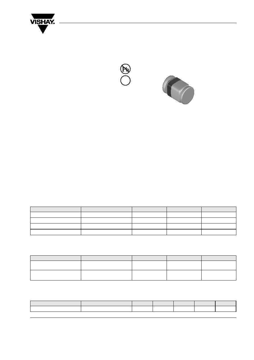
Mechanical Data
Case: MicroMELF
Weight: approx. 12 mg
Packaging codes/options:
TR / 2.5 k per 7" reel, 12.5 k/box
TR3 / 10 k per 13" reel, 10 k/box
Absolute Maximum Ratings
T
amb
= 25 °C, unless otherwise specified
Thermal Characteristics
T
amb
= 25 °C, unless otherwise specified
Electrical Characteristics
T
amb
= 25 °C, unless otherwise specified
Parameter
Test condition
Symbol
Value
Unit
Power dissipation
R
thJA
300 K/W
P
V
500
mW
Z-current
I
Z
P
V
/V
Z
mA
Junction temperature
T
j
175
°C
Storage temperature range
T
stg
- 65 to + 175
°C
Parameter
Test condition
Symbol
Value
Unit
Junction to ambient air
mounted on epoxy-glass hard
tissue, Fig. 1
R
thJA
500
K/W
Junction tie point
35 µm copper clad, 0.9 mm
2
copper area per electrode
R
thJL
300
K/W
Parameter
Test condition
Symbol
Min
Typ.
Max
Unit
Forward voltage
I
F
= 200 mA
V
F
1.5
V
e2
www.vishay.com
2
Document Number 85597
Rev. 1.9, 10-Mar-06
BZM55-Series
Vishay Semiconductors
Electrical Characteristics
BZM55C..
1)
t
p
10 ms, T/t
p
> 1000
*)
Additionnal measurement of Voltage group 9V1 to 75 at 95 % V
zmin
35 nA at T
j
25 °C
Partnumber
Zener Voltage
Range
1)
Dynamic
Resistance
Test
Current
Temperature
Coefficient
Test
Current
Reverse Leakage Current
V
Z
at I
ZT
r
zjT
at
I
ZT
,
f = 1kHz
r
zjK
at
I
ZK
,
f = 1kHz
I
ZT
TK
VZ
I
ZK
I
R
at T
amb
= 25 °C
I
R
at T
amb
= 150 °C
at V
R
V
mA
%/K
mA
µA
V
min
max
min
max
BZM55C2V4
2.28
2.56
< 85
< 600
5
- 0.09
- 0.06
1
< 50
< 100
1
BZM55C2V7
2.5
2.9
< 85
< 600
5
- 0.09
- 0.06
1
< 10
< 50
1
BZM55C3V0
2.8
3.2
< 90
< 600
5
- 0.08
- 0.05
1
< 4
< 40
1
BZM55C3V3
3.1
3.5
< 90
< 600
5
- 0.08
- 0.05
1
< 2
< 40
1
BZM55C3V6
3.4
3.8
< 90
< 600
5
-0.08
- 0.05
1
< 2
< 40
1
BZM55C3V9
3.7
4.1
< 90
< 600
5
- 0.08
- 0.05
1
< 2
< 40
1
BZM55C4V3
4
4.6
< 90
< 600
5
- 0.06
- 0.03
1
< 1
< 20
1
BZM55C4V7
4.4
5
< 80
< 600
5
- 0.05
0.02
1
< 0.5
< 10
1
BZM55C5V1
4.8
5.4
< 60
< 550
5
- 0.02
0.02
1
< 0.1
< 2
1
BZM55C5V6
5.2
6
< 40
< 450
5
- 0.05
0.05
1
< 0.1
< 2
1
BZM55C6V2
5.8
6.6
< 10
< 200
5
0.03
0.06
1
< 0.1
< 2
2
BZM55C6V8
6.4
7.2
< 8
< 150
5
0.03
0.07
1
< 0.1
< 2
3
BZM55C7V5
7
7.9
< 7
< 50
5
0.03
0.07
1
< 0.1
< 2
5
BZM55C8V2
7.7
8.7
< 7
< 50
5
0.03
0.08
1
< 0.1
< 2
6.2
BZM55C9V1 *
8.5
9.6
< 10
< 50
5
0.03
0.09
1
< 0.1
< 2
6.8
BZM55C10 *
9.4
0.6
< 15
< 70
5
0.03
0.1
1
< 0.1
< 2
7.5
BZM55C11 *
10.4
11.6
< 20
< 70
5
0.03
0.11
1
< 0.1
< 2
8.2
BZM55C12 *
11.4
12.7
< 20
< 90
5
0.03
0.11
1
< 0.1
< 2
9.1
BZM55C13 *
12.4
14.1
< 26
< 110
5
0.03
0.11
1
< 0.1
< 2
10
BZM55C15 *
13.8
15.6
< 30
< 110
5
0.03
0.11
1
< 0.1
< 2
11
BZM55C16 *
15.3
17.1
< 40
< 170
5
0.03
0.11
1
< 0.1
< 2
12
BZM55C18 *
16.8
19.1
< 50
< 170
5
0.03
0.11
1
< 0.1
< 2
13
BZM55C20 *
18.8
21.2
< 55
< 220
5
0.03
0.11
1
< 0.1
< 2
15
BZM55C22 *
20.8
23.3
< 55
< 220
5
0.04
0.12
1
< 0.1
< 2
16
BZM55C24 *
22.8
25.6
< 80
< 220
5
0.04
0.12
1
< 0.1
< 2
18
BZM55C27 *
25.1
28.9
< 80
< 220
5
0.04
0.12
1
< 0.1
< 2
20
BZM55C30 *
28
32
< 80
< 220
5
0.04
0.12
1
< 0.1
< 2
22
BZM55C33 *
31
35
< 80
< 220
5
0.04
0.12
1
< 0.1
< 2
24
BZM55C36 *
34
38
< 80
< 220
5
0.04
0.12
1
< 0.1
< 2
27
BZM55C39 *
37
41
< 90
< 500
2.5
0.04
0.12
0.5
< 0.1
< 5
30
BZM55C43 *
40
46
< 90
< 600
2.5
0.04
0.12
0.5
< 0.1
< 5
33
BZM55C47 *
44
50
110
< 700
2.5
0.04
0.12
0.5
< 0.1
< 5
36
BZM55C51 *
48
54
125
< 700
2.5
0.04
0.12
0.5
< 0.1
< 10
39
BZM55C56 *
52
60
135
< 1000
2.5
0.04
0.12
0.5
< 0.1
< 10
43
BZM55C62 *
58
66
150
< 1000
2.5
0.04
0.12
0.5
< 0.1
< 10
47
BZM55C68 *
64
72
200
< 1000
2.5
0.04
0.12
0.5
< 0.1
< 10
51
BZM55C75 *
70
79
250
< 1500
2.5
0.04
0.12
0.5
< 0.1
< 10
56
BZM55-Series
Document Number 85597
Rev. 1.9, 10-Mar-06
Vishay Semiconductors
www.vishay.com
3
Electrical Characteristics
BZM55B..
1)
t
p
10 ms, T/t
p
> 1000
*)
Additionnal measurement of Voltage group 9V1 to 75 at 95 % V
zmin
35 nA at T
j
25 °C
Partnumber
Zener Voltage
Range
1)
Dynamic
Resistance
Test
Current
Temperature
Coefficient
Test
Current
Reverse Leakage Current
V
Z
at I
ZT
r
zjT
at
I
ZT
,
f = 1kHz
r
zjK
at
I
ZK
,
f = 1kHz
I
ZT
TK
VZ
I
ZK
I
R
at
T
amb
=
25 °C
I
R
at
T
amb
=
150 °C
at V
R
V
mA
%/K
mA
µA
V
min
max
min
max
BZM55B2V4
2.35
2.45
< 85
< 600
5
- 0.09
- 0.06
1
< 50
< 100
1
BZM55B2V7
2.64
2.76
< 85
< 600
5
- 0.09
- 0.06
1
< 10
< 50
1
BZM55B3V0
2.94
3.06
< 90
< 600
5
- 0.08
- 0.05
1
< 4
< 40
1
BZM55B3V3
3.24
3.36
< 90
< 600
5
- 0.08
- 0.05
1
< 2
< 40
1
BZM55B3V6
3.52
3.68
< 90
< 600
5
- 0.08
- 0.05
1
< 2
< 40
1
BZM55B3V9
3.82
3.98
< 90
< 600
5
- 0.08
- 0.05
1
< 2
< 40
1
BZM55B4V3
4.22
4.38
< 90
< 600
5
- 0.06
- 0.03
1
< 1
< 20
1
BZM55B4V7
4.6
4.80
< 80
< 600
5
- 0.05
0.02
1
< 0.5
< 10
1
BZM55B5V1
5
5.20
< 60
< 550
5
- 0.02
0.02
1
< 0.1
< 2
1
BZM55B5V6
5.48
5.72
< 40
< 450
5
- 0.05
0.05
1
< 0.1
< 2
1
BZM55B6V2
6.08
6.32
< 10
< 200
5
0.03
0.06
1
< 0.1
< 2
2
BZM55B6V8
6.66
6.94
< 8
< 150
5
0.03
0.07
1
< 0.1
< 2
3
BZM55B7V5
7.35
7.65
< 7
< 50
5
0.03
0.07
1
< 0.1
< 2
5
BZM55B8V2
8.04
8.36
< 7
< 50
5
0.03
0.08
1
< 0.1
< 2
6.2
BZM55B9V1 *
8.92
9.28
< 10
< 50
5
0.03
0.09
1
< 0.1
< 2
6.8
BZM55B10 *
9.8
10.20
< 15
< 70
5
0.03
0.1
1
< 0.1
< 2
7.5
BZM55B11 *
10.78
11.22
< 20
< 70
5
0.03
0.11
1
< 0.1
< 2
8.2
BZM55B12 *
11.76
12.24
< 20
< 90
5
0.03
0.11
1
< 0.1
< 2
9.1
BZM55B13 *
12.74
13.26
< 26
< 110
5
0.03
0.11
1
< 0.1
< 2
10
BZM55B15 *
14.7
15.30
< 30
< 110
5
0.03
0.11
1
< 0.1
< 2
11
BZM55B16 *
15.7
16.30
< 40
< 170
5
0.03
0.11
1
< 0.1
< 2
12
BZM55B18 *
17.64
18.36
< 50
< 170
5
0.03
0.11
1
< 0.1
< 2
13
BZM55B20 *
19.6
20.40
< 55
< 220
5
0.03
0.11
1
< 0.1
< 2
15
BZM55B22 *
21.55
22.45
< 55
< 220
5
0.04
0.12
1
< 0.1
< 2
16
BZM55B24 *
23.5
24.5
< 80
< 220
5
0.04
0.12
1
< 0.1
< 2
18
BZM55B27 *
26.4
27.6
< 80
< 220
5
0.04
0.12
1
< 0.1
< 2
20
BZM55B30 *
29.4
30.6
< 80
< 220
5
0.04
0.12
1
< 0.1
< 2
22
BZM55B33 *
32.4
33.6
< 80
< 220
5
0.04
0.12
1
< 0.1
< 2
24
BZM55B36 *
35.3
36.7
< 80
< 220
5
0.04
0.12
1
< 0.1
< 2
27
BZM55B39 *
38.2
39.8
< 90
< 500
2.5
0.04
0.12
1
< 0.1
< 5
30
BZM55B43 *
42.1
43.9
< 90
< 600
2.5
0.04
0.12
0.5
< 0.1
< 5
33
BZM55B47 *
46.1
47.9
< 110
< 700
2.5
0.04
0.12
0.5
< 0.1
< 5
36
BZM55B51 *
50
52.0
< 125
< 700
2.5
0.04
0.12
0.5
< 0.1
< 10
39
BZM55B56 *
54.9
57.1
< 135
< 1000
2.5
0.04
0.12
0.5
< 0.1
< 10
43
BZM55B62 *
60.8
63.2
< 150
< 1000
2.5
0.04
0.12
0.5
< 0.1
< 10
47
BZM55B68 *
66.6
69.4
< 200
< 1000
2.5
0.04
0.12
0.5
< 0.1
< 10
51
BZM55C75 *
73.5
76.5
< 250
< 1500
2.5
0.04
0.12
0.5
< 0.1
< 10
56
www.vishay.com
4
Document Number 85597
Rev. 1.9, 10-Mar-06
BZM55-Series
Vishay Semiconductors
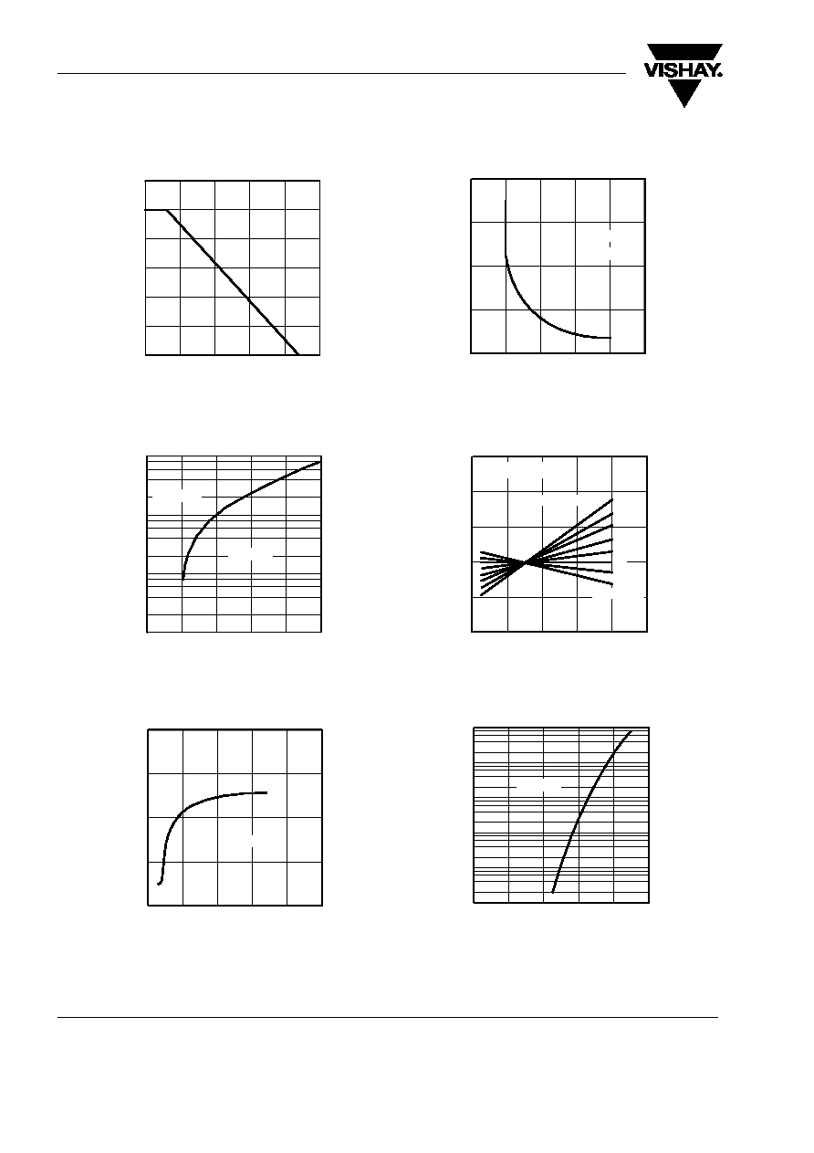
Typical Characteristics
T
amb
= 25 °C, unless otherwise specified
Figure 1. Total Power Dissipation vs. Ambient Temperature
Figure 2. Typical Change of Working Voltage under Operating
Conditions at T
amb
=25°C
Figure 3. Temperature Coefficient of Vz vs. Z-Voltage
0
120
160
0
100
300
400
500
600
P
tot
- Total Po
w
er Dissipation (m
W
)
T
amb
- Ambient Temperature (°C)
200
95 9602
200
80
40
10
15
20
1
10
100
1000
V
Z
-
V
oltage Change (m
V
)
V
Z
- Z-Voltage (V)
25
95 9598
T
j
= 25 °C
I
Z
= 5 mA
0
5
30
- 5
0
5
10
15
V
Z
- Z-Voltage (V)
50
95 9600
40
I
Z
= 5 mA
10
20
0
TK
V
Z
-
T
emper
at
u
re Coefficient of
V
Z
(10
-4
/K)
Figure 4. Diode Capacitance vs. Z-Voltage
Figure 5. Typical Change of Working Voltage vs. Junction
Temperature
Figure 6. Forward Current vs. Forward Voltage
10
15
0
50
100
150
200
C
D
- Diode Capacitance (pF)
V
Z
- Z-Voltage (V)
25
95 9601
20
T
j
= 25 °C
V
R
= 2 V
0
5
- 60
60
120
180
0.8
0.9
1.0
1.1
1.2
1.3
V
Ztn
- Relati
v
e
V
oltage Change
T
j
- Junction Temperature (°C)
240
95 9599
0
V
Ztn
= V
Zt
/V
Z
(25 °C)
0
TK
VZ
= 10 x 10
-4
/K
8 x 10
-4
/K
2 x 10
-4
/K
6 x 10
-4
/K
4 x 10
-4
/K
- 4 x 10
-4
/K
- 2 x 10
-4
/K
0
0.2
0.4
0.6
0.8
0.001
0.01
0.1
1
10
100
1.0
95 9605
I
F
- For
w
ard C
u
rrent (mA)
V
F
- Forward Voltage (V)
T
j
= 25 °C
BZM55-Series
Document Number 85597
Rev. 1.9, 10-Mar-06
Vishay Semiconductors
www.vishay.com
5
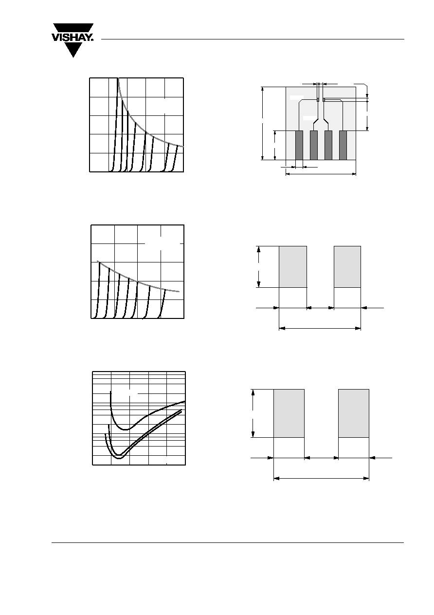
Figure 7. Z-Current vs. Z-Voltage
Figure 8. Z-Current vs. Z-Voltage
Figure 9. Differential Z-Resistance vs. Z-Voltage
8
20
95 9604
0
20
40
60
80
100
I
Z
- Z-C
u
rrent (mA)
P
tot
= 500 mW
T
amb
= 25 °C
0
4
6
12
V
Z
- Z-Voltage (V)
15
20
25
30
0
10
20
30
40
50
I
Z
- Z-C
u
rrent (mA)
V
Z
- Z-Voltage (V)
35
95 9607
P
tot
= 500 mW
T
amb
= 25 °C
0
5
10
15
20
1
10
100
1000
(
)
25
95 9606
Tj = 25 °C
I
Z
= 1 mA
5 mA
10 mA
V
Z
- Z-Voltage (V)
r
Z
- Diff
erential Z-Resistance
Figure 10. Board for R
thJA
definition (in mm)
Figure 11. Recommended foot pads (in mm)
Figure 12. Recommended foot pads (in mm)
25
2.5
10
0.71
1.3
1.27
9.9
24
0.152
0.355
95 10329
1.2
0.8
2.4
0.8
0.8
16773
Reflow Soldering
1.4
1.0
2.8
0.9
0.9
Wave Soldering
16774