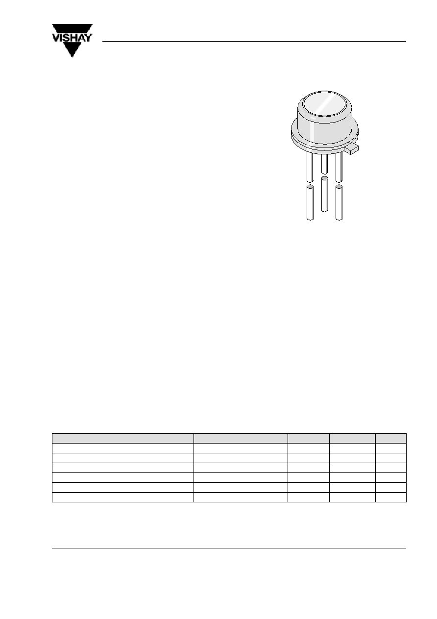
BPW97
Vishay Telefunken
1 (6)
Rev. 2, 20-May-99
www.vishay.de
·
FaxBack +1-408-970-5600
Document Number 81533
Silicon PIN Photodiode
Description
BPW97 is an extra high speed PIN photodiode in a
hermetically sealed TO18 package.
Unlike most similar devices, the cathode terminal is
isolated from case and connected to a third terminal,
giving the user all the means to improve shielding of his
system.
Due to its high precision flat glass window and its accu-
rate chip alignment, this device is recommended for
ambitious applications in the optical data transmission
domain.
Features
D
Extra fast response times at low operating volt-
ages
D
Exact central chip alignment
D
Chip insulated
D
Shielded construction
D
Hermetically sealed TO18 case
D
Flat optical window
D
Wide angle of half sensitivity
=
±
55
°
D
Radiant sensitive area A=0.25mm
2
D
Suitable for visible and near infrared radiation
D
Suitable for coupling with 50
m
m gradient index fi-
ber
94 8478
Applications
Wide band detector for demodulation of fast signals, e.g. of lasers and GaAs emitters.
Detector for optical communication, e.g. for optical fiber transmission systems with only 5 V power supply.
Absolute Maximum Ratings
T
amb
= 25
_
C
Parameter
Test Conditions
Symbol
Value
Unit
Reverse Voltage
V
R
60
V
Power Dissipation
T
amb
x
25
°
C
P
V
285
mW
Junction Temperature
T
j
125
°
C
Storage Temperature Range
T
stg
55...+125
°
C
Soldering Temperature
t
x
5 s
T
sd
260
°
C
Thermal Resistance Junction/Ambient
R
thJA
350
K/W

BPW97
Vishay Telefunken
2 (6)
Rev. 2, 20-May-99
www.vishay.de
·
FaxBack +1-408-970-5600
Document Number 81533
Basic Characteristics
T
amb
= 25
_
C
Parameter
Test Conditions
Symbol
Min
Typ
Max
Unit
Forward Voltage
I
F
= 50 mA
V
F
0.9
1.2
V
Breakdown Voltage
I
R
= 100
m
A, E = 0
V
(BR)
60
V
Reverse Dark Current
V
R
= 50 V, E = 0
I
ro
1
5
nA
Diode Capacitance
V
R
= 50 V, f = 1 MHz, E = 0
C
D
1.7
pF
Dark Resistance
V
R
= 10m V, E = 0, f = 0
R
D
5
G
W
Serial Resistance
V
R
= 50 V, f = 1 MHz
R
S
180
W
Reverse Light Current
E
e
= 1 mW/cm
2
,
l
= 870 nm, V
R
= 50 V
I
ra
1.0
1.3
m
A
E
e
= 1 mW/cm
2
,
l
= 950 nm, V
R
= 50 V
I
ra
0.9
m
A
Temp. Coefficient of I
ra
V
R
= 50 V,
l
= 870 nm
TK
Ira
0.2
%/K
Absolute Spectral Sensitivity
V
R
= 5 V,
l
= 870 nm
s(
l
)
0.50
A/W
y
V
R
= 5 V,
l
= 950 nm
s(
l
)
0.35
A/W
Angle of Half Sensitivity
±
55
deg
Wavelength of Peak Sensitivity
l
p
810
nm
Range of Spectral Bandwidth
l
0.5
560...960
nm
Quantum Efficiency
l
= 850 nm
h
80
%
Noise Equivalent Power
V
R
= 50 V,
l
= 870 nm
NEP
3.6x10
14
W/
Hz
Detectivity
V
R
= 50 V,
l
= 870 nm
D
*
1.4x10
12
cm
Hz/
W
Rise Time
V
R
= 3.8 V, R
L
= 50
W
,
l
= 780 nm
t
r
1.2
ns
Fall Time
V
R
= 3.8 V, R
L
= 50
W
,
l
= 780 nm
t
f
1.2
ns
Rise Time
V
R
= 50 V, R
L
= 50
W
,
l
= 820 nm
t
r
0.6
ns
Fall Time
V
R
= 50 V, R
L
= 50
W
,
l
= 820 nm
t
f
0.6
ns
CutOff Frequency
l
= 820 nm
f
c
1
GHz
BPW97
Vishay Telefunken
3 (6)
Rev. 2, 20-May-99
www.vishay.de
·
FaxBack +1-408-970-5600
Document Number 81533
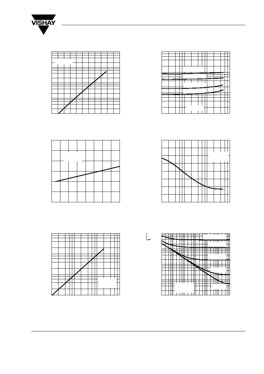
Typical Characteristics (T
amb
= 25
_
C unless otherwise specified)
40
60
80
120
94 8445
100
20
I Reverse Dark Current ( nA
)
ro
T
amb
Ambient Temperature (
°
C )
10
0
10
1
10
2
10
3
10
4
V
R
=50V
Figure 1. Reverse Dark Current vs. Ambient Temperature
0.8
0.9
1.0
1.1
1.2
1.4
1.3
I Relative Reverse Light Current
ra rel
T
amb
Ambient Temperature (
°
C )
94 8446
20
40
60
80
100
V
R
=50V
l=870nm
Figure 2. Relative Reverse Light Current vs.
Ambient Temperature
0.01
0.1
1
10
0.01
0.1
1
I Reverse Light Current (
A
)
ra
E
e
Irradiance ( mW / cm
2
)
10
94 8447
m
V
R
=50V
l=950nm
Figure 3. Reverse Light Current vs. Irradiance
0.01
0.1
1
10
94 8448
I Reverse Light Current (
A
)
ra
m
0.1
1
10
V
R
Reverse Voltage ( V )
100
1 mW/cm
2
0.5 mW/cm
2
0.2 mW/cm
2
0.1 mW/cm
2
l=950nm
Figure 4. Reverse Light Current vs. Reverse Voltage
0
2
4
6
8
0.1
1
10
C Diode Capacitance ( pF )
D
V
R
Reverse Voltage ( V )
100
94 8449
E=0
f=1MHz
Figure 5. Diode Capacitance vs. Reverse Voltage
NEP
Noise Equivalent Power (
W
/ Hz )
R
L
Load Resistance (
W )
94 8450
10
2
10
3
10
4
10
5
10
6
10
7
10
8
10
14
10
13
10
12
10
11
10
10
f=1000MHz
500MHz
100MHz
10MHz
1MHz
f;B=1
l=870nm
Figure 6. Noise Equivalent Power vs. Load Resistance

BPW97
Vishay Telefunken
4 (6)
Rev. 2, 20-May-99
www.vishay.de
·
FaxBack +1-408-970-5600
Document Number 81533
1
10
100
3
2
1
0
1
3
S ( , ) Relative Sensitivity ( dB )
rel
f Frequency ( MHz )
1000
94 8451
2
l
V
R
=50V
15V
Figure 7. Relative Sensitivity vs. Frequency
350
550
750
950
0
0.2
0.4
0.6
0.8
1.0
1150
94 8452
S ( ) Relative Spectral Sensitivity
rel
l Wavelength ( nm )
l
Figure 8. Relative Spectral Sensitivity vs. Wavelength
0.4
0.2
0
0.2
0.4
S Relative Sensitivity
rel
0.6
94 8453
0.6
0.9
0.8
0
°
30
°
10
°
20
°
40
°
50
°
60
°
70
°
80
°
0.7
1.0
Figure 9. Relative Radiant Sensitivity vs.
Angular Displacement

BPW97
Vishay Telefunken
5 (6)
Rev. 2, 20-May-99
www.vishay.de
·
FaxBack +1-408-970-5600
Document Number 81533
Dimensions in mm
96 12182