Äîêóìåíòàöèÿ è îïèñàíèÿ www.docs.chipfind.ru
VISHAY
BC856 to BC859
Document Number 85135
Rev. 1.2, 08-Sep-04
Vishay Semiconductors
www.vishay.com
1
1
3
2
E
B
C
3
1
2
18978
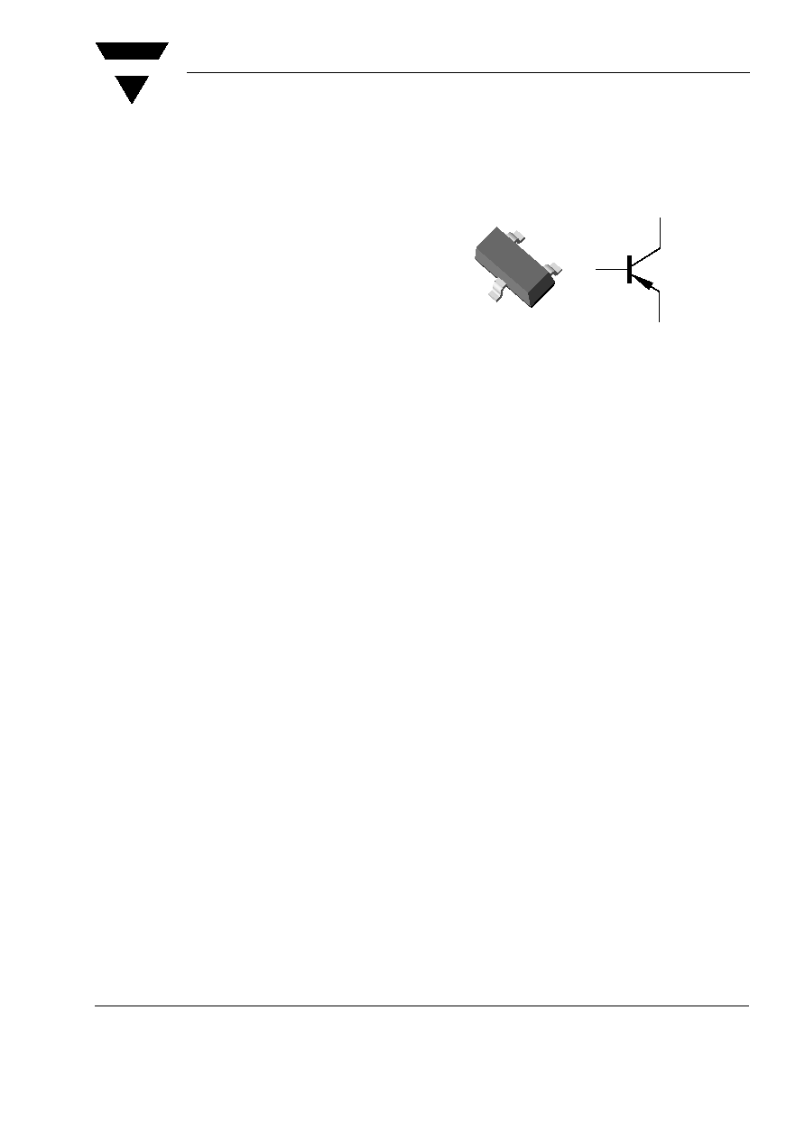
Small Signal Transistors (PNP)
Features
· PNP Silicon Epitaxial Planar Transistors for
switching and AF amplifier applications.
· Especially suited for automatic insertion in thick
and thin-film circuits.
· These transistors are subdivided into three groups
A, B, and C) according to their current gain. The
type BC856 is available in groups A and B, how-
ever, the types
BC857, BC558 and BC859 can be supplied in all
three groups. The BC849 is a low noise type.
· As complementary types, the NPN transistors
BC846...BC849 are recomended.
Mechanical Data
Case: SOT-23 Plastic case
Weight: approx. 8.8 mg
Marking:
BC856A = 3A BC858A = 3J
BC856B = 3B BC858B = 3K
BC858C = 3L
BC857A = 3E BC859A = 4A
BC857B = 3F BC859B = 4B
BC857C = 3G BC859C = 4C
Packaging Codes/Options:
GS18 / 10 k per 13" reel (8 mm tape), 10 k/box
GS08 / 3 k per 7" reel (8 mm tape), 15 k/box
Pinning:
1 = Base, 2 = Emitter, 3 = Collector
www.vishay.com
2
Document Number 85135
Rev. 1.2, 08-Sep-04
VISHAY
BC856 to BC859
Vishay Semiconductors
Absolute Maximum Ratings
T
amb
= 25 °C, unless otherwise specified
1)
Device on fiberglass substrate, see layout on third page.
Maximum Thermal Resistance
1)
Device on fiberglass substrate, see layout on third page.
Electrical DC Characteristics
Parameter
Test condition
Part
Symbol
Value
Unit
Collector - base voltage
BC856
- V
CBO
80
V
BC857
- V
CBO
50
V
BC858
- V
CBO
30
V
BC859
- V
CBO
30
V
Collector - emitter voltage
(base shorted)
BC856
- V
CES
80
V
BC857
- V
CES
50
V
BC858
- V
CES
30
V
BC859
- V
CES
30
V
Collector - emitter voltage
(base open)
BC856
- V
CEO
65
V
BC857
- V
CEO
45
V
BC858
- V
CEO
30
V
BC859
- V
CEO
30
V
Emitter - base voltage
- V
EBO
5
V
Collector current
- I
C
100
mA
Peak colector current
- I
CM
200
mA
Peak base current
- I
BM
200
mA
Peak emitter current
I
EM
200
mA
Power dissipation
T
amb
= 25 °C
P
tot
310
1)
mW
Parameter
Test condition
Symbol
Value
Unit
Thermal resistance junction to
ambient air
R
JA
320
1)
°C/W
Thermal resistance junction to
substrate backside
R
SB
450
1)
°C/W
Junction temperature
T
j
150
°C
Storage temperature range
T
S
- 65 to + 150
°C
Parameter
Test condition
Part
Symbol
Min
Typ
Max
Unit
Small signal current gain
(current gain group A)
- V
CE
= 5 V, - I
C
= 2 mA, f = 1 kHz
h
fe
220
Small signal current gain
(current gain group B)
- V
CE
= 5 V, - I
C
= 2 mA, f = 1 kHz
h
fe
330
Small signal current gain
(current gain group C)
- V
CE
= 5 V, - I
C
= 2 mA, f = 1 kHz
h
fe
600
Input impedance (current gain
group A)
- V
CE
= 5 V, - I
C
= 2 mA, f = 1 kHz
h
ie
1.6
2.7
4.5
k
Input impedance (current gain
group B)
- V
CE
= 5 V, - I
C
= 2 mA, f = 1 kHz
h
ie
3.2
4.5
8.5
k
Input impedance (current gain
group C)
- V
CE
= 5 V, - I
C
= 2 mA, f = 1 kHz
h
ie
6
8.7
15
k
Output admittance (current gain
group A)
- V
CE
= 5 V, - I
C
= 2 mA, f = 1 kHz
h
oe
18
30
µS

VISHAY
BC856 to BC859
Document Number 85135
Rev. 1.2, 08-Sep-04
Vishay Semiconductors
www.vishay.com
3
Output admittance (current gain
group B)
- V
CE
= 5 V, - I
C
= 2 mA, f = 1 kHz
h
oe
30
60
µS
Output admittance (current gain
group C)
- V
CE
= 5 V, - I
C
= 2 mA, f = 1 kHz
h
oe
60
110
µS
Reverse voltage transfer ratio
(current gain group A)
- V
CE
= 5 V, - I
C
= 2 mA, f = 1 kHz
h
re
1.5 x 10
-4
Reverse voltage transfer ratio
(current gain group B)
- V
CE
= 5 V, - I
C
= 2 mA, f = 1 kHz
h
re
2 x 10
-4
Reverse voltage transfer ratio
(current gain group C)
- V
CE
= 5 V, - I
C
= 2 mA, f = 1 kHz
h
re
3 x 10
-4
DC current gain (current gain
group A)
- V
CE
= 5 V, - I
C
= 10
µA
h
FE
90
DC current gain (current gain
group B)
- V
CE
= 5 V, - I
C
= 10
µA
h
FE
150
DC current gain (current gain
group C)
- V
CE
= 5 V, - I
C
= 10
µA
h
FE
270
DC current gain (current gain
group A)
- V
CE
= 5 V, - I
C
= 2 mA
h
FE
110
180
220
DC current gain (current gain
group B)
- V
CE
= 5 V, - I
C
= 2 mA
h
FE
200
290
450
DC current gain (current gain
group C)
- V
CE
= 5 V, - I
C
= 2 mA
h
FE
420
520
800
Collector saturation voltage
- I
C
= 10 mA, - I
B
= 0.5 mA
V
CEsat
90
300
mV
- I
C
= 100 mA, - I
B
= 5 mA
V
CEsat
250
650
mV
Base saturation voltage
- I
C
= 10 mA, - I
B
= 0.5 mA
V
BEsat
700
mV
- I
C
= 100 mA, - I
B
= 5 mA
V
BEsat
900
mV
Base - emiter voltage
- V
CE
= 5 V, - I
C
= 2 mA
V
BE
600
660
750
mV
- V
CE
= 5 V, - I
C
= 10 mA
V
BE
820
mV
Collector-emitter cut-off current
- V
CE
= 80 V
BC856
I
CES
0.2
15
nA
- V
CE
= 50 V
BC857
I
CES
0.2
15
nA
- V
CE
= 30 V
BC858
I
CES
0.2
15
nA
BC859
I
CES
0.2
15
nA
- V
CE
= 80 V, T
j
= 125 °C
BC857
I
CES
4
µA
- V
CE
= 50 V, T
j
= 125 °C
BC857
I
CES
4
µA
- V
CE
= 30 V, T
j
= 125 °C
BC858
I
CES
4
µA
BC859
I
CES
4
µA
Collector-base cut-off current
- V
CB
= 30 V
I
CBO
15
µA
- V
CB
= 30 V, T
j
= 150 °C
I
CBO
5
µA
Parameter
Test condition
Part
Symbol
Min
Typ
Max
Unit
www.vishay.com
4
Document Number 85135
Rev. 1.2, 08-Sep-04
VISHAY
BC856 to BC859
Vishay Semiconductors
Electrical AC Characteristics
Parameter
Test condition
Part
Symbol
Min
Typ
Max
Unit
Gain bandwidth product
- V
CE
= 5 V, - I
C
= 10 mA,
f = 100 MHz
f
T
150
MHz
Collector - base capacitance
- V
CB
= 10 V, f = 1 MHz
C
CBO
6
pF
Noise figure
- V
CE
= 5 V, - I
C
= 200
µA,
R
G
= 2 k
, f = 1 kHz,
f = 200 Hz
BC856
F
2
10
dB
BC857
F
2
10
dB
BC858
F
2
10
dB
BC859
F
1
4
dB
- V
CE
= 5 V, - I
C
= 200
µA,
R
G
= 2 k
,
f = (30 to 15000) Hz
BC859
F
1.2
4
dB
VISHAY
BC856 to BC859
Document Number 85135
Rev. 1.2, 08-Sep-04
Vishay Semiconductors
www.vishay.com
5
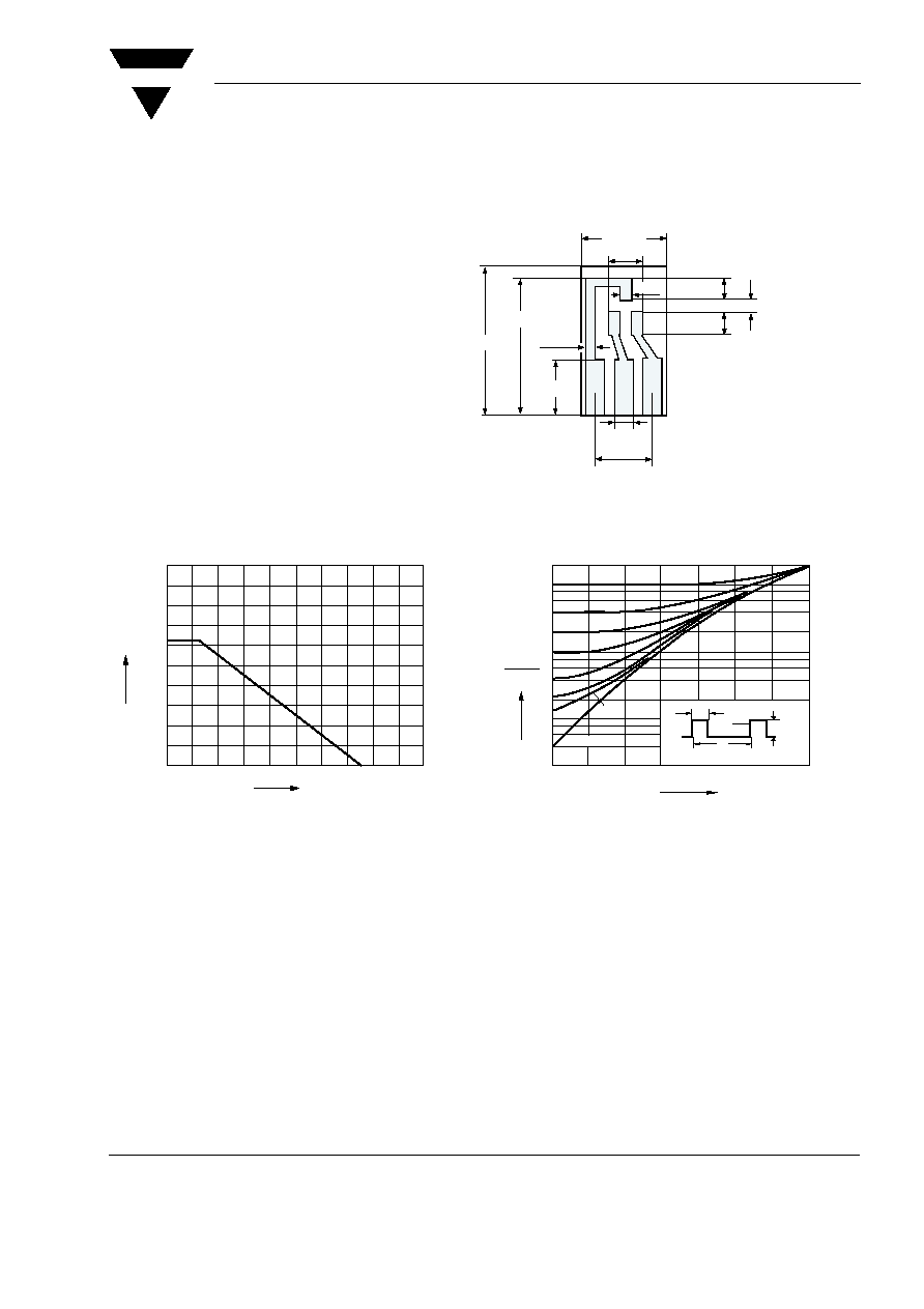
Layout for R
thJA
test
Thickness: Fiberglass 1.5 mm (0.059 in.)
Copper leads 0.3 mm (0.012 in.)
Typical Characteristics
(T
amb
= 25
°C unless otherwise specified)
17451
15 (0.59)
12 (0.47)
0.8 (0.03)
5 (0.2)
7.5 (0.3)
3 (0.12)
1 (0.4)
1 (0.4)
2 (0.8)
2 (0.8)
1.5 (0.06)
5.1 (0.2)
Figure 1. Admissible Power Dissipation vs. Temperature of
Substrate Backside
mW
500
400
300
200
100
0
0
100
200 °C
Ptot
TSB
19195
Figure 2. Pulse Thermal Resistance vs. Pulse Duration
(normalized)
-1
10
10
1s
10
10
10
10
10
10
-1
-2
-3
-4
-5
-6
tp
t
p
tp
P
I
T
T
=
0.2
0.5
0.1
0.05
0.02
0.01
0.005
= 0
10
-7
-2
10
-3
10
rthSB
R thSB
19191
Document Outline