
UTC MC34118
LINEAR INTEGRATED CIRCUIT
UTC
UNISONIC TECHNOLOGIES CO., LTD.
1
QW-R108-007,A
VOICE SWITCHED
SPEAKER-PHONE CIRCUIT
DESCRIPTION
The UTC MC34118 voice switched speaker-phone
integrated circuit incorporates the necessary amplifiers,
attenuators, level detectors and control algorithm to form the
heart of a high quality hands-free speaker-phone system. It
includes a microphone amplifier with adjustable gain and
mute control. Transmit and Receive attenuators which
operate in a complementary manner, level detectors at both
input and output of both attenuators, and background noise
monitors for both the transmit and receive channels. A dial
tone detector prevents the dial tone from being attenuated by
the receive background noise monitor circuit. Also two line
driver amplifiers which can be used to form a hybrid network
in conjunction with an external coupling transformer. A
high-pass filter can be used to filter out 60Hz noise in the
receive channel, or for other filtering functions. A chip disable
pin permits powers down the entire circuit to converse power
on long loops where loop current is at a minimum. The UTC
MC34118 may be operated from a power supply, or it can be
powered from the telephone line, requiring typically 5mA. The
UTC MC34118 can be interfaced directly to TIP and
RING( through a coupling transformer) for stand-alone
operation, or it can be used in conjunction with a handset
speech network and/or other features of a feature phone.
FEATURES
*Improved attenuator gain range: 52dB between Transmit
and Receive
*Low voltage operation for line-powered applications(3~6.5V)
*4-point signal sensing for improved sensitivity
*Background noise monitors for both Transmit and Receive
paths
DIP-28
SOP-28
*Microphone amplifier gain set by external
Resistors-Mute function included
*Chip disable for active/standby operation
*On board filter pinned-out for user defined
function
*Dial tone detector to inhibit receive idle mode
during dial tone presence
ABSOLUTE MAXIMUM RATINGS
(Ta=25
�C
,Voltages referred to pin 22
)
PARAMETER SYMBOL
VALUE
UNIT
Supply Voltage
Vcc
-1~7
V
Voltage at Pin 3
V3
-1~Vcc+1
V
Voltage at Pin 12( mute)
V12
-1~Vcc+1
V
Voltage at Pin 13( VLC)
V13
-1~Vcc+0.5
V
Voltage at Pin 9, Pin 21, and Pin 2
V9, 21, 2
-0.5~Vcc+0.5
V
Storage temperature
Tstr
-65~150
�C
UTC MC34118
LINEAR INTEGRATED CIRCUIT
UTC
UNISONIC TECHNOLOGIES CO., LTD.
2
QW-R108-007,A
RECOMMENDED OPERATION CONDITIONS
PARAMETER SYMBOL
VALUE
UNIT
Supply Voltage
V4
3.5~6.5
V
Voltage at Pin 3
V3
0~Vcc
V
Voltage at Pin 12( MUTE)
V12
0~Vcc
V
Voltage at Pin 13( VLC)
V13
0.3*VB~VB
V
IVB Current( Pin 15)
I
VB
500
�A
Attenuator Input Signal Voltage at Pin 9, Pin 21
V9, V21
350
Mvrms
Load Current
@RXO, TXO(Pin8, Pin 22)
@MCO(Pin 10)
@HTO-, HTO+(Pin 6, Pin5)
0~+-2
0~+-1
0~+-0.5
mA
Ambient Operating Temperature
Topr
-20~60
�C
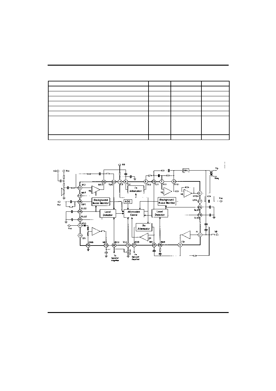
BLOCK DIAGRAM

UTC MC34118
LINEAR INTEGRATED CIRCUIT
UTC
UNISONIC TECHNOLOGIES CO., LTD.
3
QW-R108-007,A
PIN CONFIGURATIONS
PIN NAME
DESCRIPTION
1
FO
Filter Output. Output impedance is less than 50 ohms.
2
FI
Filter Input. Input impedance is greater than 1 M ohms.
3
CD
Chip Disable. A logic low (<0.8V) sets normal operation. A logic high (>2V) disable the IC to converse
power. Input impedance is nominally 90 K ohms.
4 Vcc
A supply voltage of +2.8V to +6.5V is required at 5mA. As Vcc falls from 3.5V to 2.8V, an AGC circuit
reduces the receive attenuator gain by 25dB( when in the receive mode).
5
HTO+ Output of the second hybrid amplifier. The gain is internally set at -1 to provide a differential output, in
conjunction with HTO-, to the hybrid transformer.
6
HTO- Output of the first hybrid amplifier. The gain of the amplifier is set by external resistors.
7
HTI Input and summing node for the first hybrid amplifier. DC lever is about equal to VB.
8
TXO Output of the transmit attenuator. DC level is about VB.
9 TXI
Input of the transmit attenuator. Maximum signal level is 350 mVrms. Input impedance is 10K
.
10
MCO Output of the microphone amplifier. The gain of the amplifier is set by external resistors.
11
MCI Input of the summing node of the microphone. DC lever is VB.
12
MUT Mute input. A logic low (<0.8V) sets normal operation. A logic high (>2V) mutes the microphone
amplifier without affecting the rest of the circuit. Input impedance is 90 K ohms.
13
VLC Volume control input. When VLC=VB, the receive attenuator is at maximum gain when in the receive
mode. When VLC=0.3dB, the receive gain is down 35dB. Does not effect the transmit modes.
14
CT
The RC at this pin sets the response time for the circuit to switch modes.
15
VB
N output voltage=Vcc/2. This voltage is a system AC ground and biases the volume control. A filter
capacitor is required.
16
CPT The RC at this pin sets the time constant for the transmit background side.
17
TLI2 Input to the transmit level detector on the microphone/ speaker side.
18 TLO2 Output to the transmit level detector on the microphone/ speaker side, and input to the transmit
background monitor.
19 RLO2 Output of the receive level detector on the microphone/ speaker side
20
RLI2 Input to the receive level detector on the microphone/ speaker side
21
RXI Input to the receive attenuator and dial tone detector. Maximum input level is 350mVrms. Input
impedance is 10K
.
22
RXO Output of the receive attenuator. DC level is VB.
23
TLI1 Input to the transmit level detector on the line side.
24 TLO1 Output to the transmit level detector on the line side, and input to the transmit background monitor.
25 RLO1 Output of the receive level detector on the line side.
26
RLI1 Input to the receive level detector on the line side.
27
CPR The RC at this pin sets the time constant for the receive background monitor.
28
GND Ground pin for the entire IC.

UTC MC34118
LINEAR INTEGRATED CIRCUIT
UTC
UNISONIC TECHNOLOGIES CO., LTD.
4
QW-R108-007,A
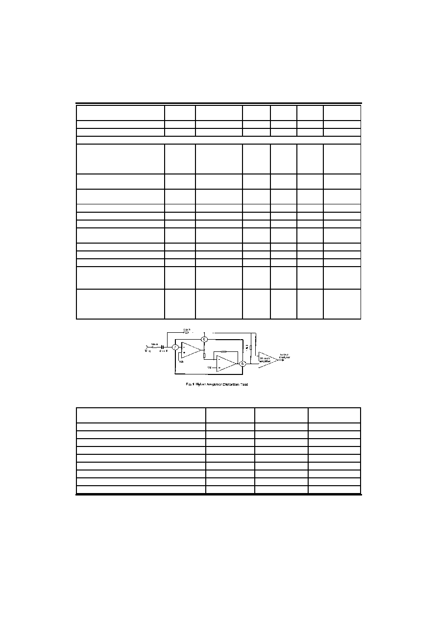
ELECTRICAL CHARACTERISTICS
(referred to fig. 1)
PARAMETER SYMBOL
TEST
CONDITIONS
MIN TYP MAX UNIT
SUPPLY VOLTAGES
V+ Supply Current
Vcc=6.5V, CD=0.8V
Vcc=6.5V, CD=2V
I
cc
5.5
600
8
800
mA
�A
CD Input Resistance
R
CD
Vcc=V
CD
=6.5V
50 90
k
CD Input Voltage(High)
V
CDH
2
Vcc
V
CD Input Voltage
V
CDL
0.8
V
V
B
Output Voltage
V
B
Vcc=3.5V
Vcc=5V
1.8
1. 3
2.1
2.4
V
V
B
Output Resistance
R
OVB
I
VB
=1mA
400
V
B
Power Supply Rejection Ratio
PSRR
C
VB
=220
�F,
f=1kHz
54 dB
ATTENUATORS
Receive Attenuator Gain(f=1kHz, V
LC
=V
B
)
Rx Mode, RXI=150mVrms
G
RX
Vcc=5V 4 6 8 dB
Rx Mode, RXI=150mVrms
G
RX
Vcc=3.5V 4 6 8 dB
Gain Change
G
RX1
Vcc=3.5V vs.
Vcc=5V
-0.5 0 +0.5 dB
AGC Gain Change
G
RX2
Vcc=3.5V vs.
Vcc=5V
-25
-15 dB
Idle Mode, RXI=150mVrms
G
RXI
-22
-20
-17
dB
Rx to Tx Mode Range
G
RX3
49
52
54
dB
Volume Control Range
V
CR
27
35
dB
RXO DC Voltage
V
RXO
Rx
Mode VB
V
RXO DC Voltage
V
RXO
Rx to Tx Mode
+-10
+-150
mV
RXO High Voltage
V
RXOH
Iout=-1mA,
RXI=V
B
+1.5V
3.7
V
RXO Low Voltage
V
RXOL
Iout=+1mA,
RXI=V
B
-1V,
Output Measured
with Respect to
V
B
-1.5
-1 V
RXI Input Resistance
R
RXI
RXI<350mVrs
7
10 14
k
TRANSMIT ATTENUATOR GAIN(f=1kHz)
Tx Mode, TXI=150mVrms
G
TX
4
6
8
dB
Idle Mode, TXI=150mVrms
G
TXI
-22
-20
-17
dB
Tx to Rx Mode Range
G
TXI
49
52
54
dB
TXO DC Voltage
V
TXO
Tx
V
B
V
TXO DC Voltage
V
TXO
Tx to Rx Mode
+-30
+-150
mV
TXO High Voltage
V
TXOH
Iout=-1mA,
TXI=V
B
+1.5V
3.7
V
UTC MC34118
LINEAR INTEGRATED CIRCUIT
UTC
UNISONIC TECHNOLOGIES CO., LTD.
5
QW-R108-007,A
PARAMETER SYMBOL
TEST
CONDITIONS
MIN TYP MAX UNIT
TXO Low Voltage
V
TXOL
Iout=+1mA,
TXI=V
B
-1V,
Output Measured
with Respect to
V
B
-1.5
-1 V
TXI Input Resistance
R
TXI
TXI<350mVrs
7 10 14
k
Gain Tracking
G
TR
GRx+GTx,
@Tx,
Idle, Rx
+-0.1
dB
ATTENUATOR CONTROL
CT Voltage( CT-V
B
)
Rx Mode
V
LC
=V
B
240
mV
Idle Mode
0
mV
Tx Mode
-240
mV
CT Source Current
I
CTR
(Switching
to
Rx Mode)
-85 -60 -40
�A
CT Sink Current
I
CTT
(Switching
to
Tx Mode)
+40 +60 +85
�A
CT Slow Idle Current
I
CTS
0
�A
CT Fast Idle Internal Resistance
R
FI
1.5
2
3.6
k
VLC Input Current
I
VLC
-60
nA
Dial Tone Detector Threshold
V
DT
10
15
20
mV
MICROPHONE AMPLIFIER( V
MUT<
0.8V, A
VCL
=31dB, unless otherwise specified)
Output Offset
M
COVOS
V
MCO-
V
B,
Rf
=180k
-50 0 50 mV
Open Loop Gain
A
VOLM
F<100Hz 70 80
dB
Gain Bandwidth
G
BWM
1
MHz
Output High Voltage
V
MCOH
Iout=1mA,
Vcc=5V
3.7
V
Output Low Voltage
V
MCOL
Iout=1mA
200 mV
Input Bias Current
I
BM
@MCI
-40
nA
Muting(
Gain)
G
MT
f=1kHz,
V
MUT
=2V
300Hz<f<10kHz
-55
-68
dB
MUT Input Resistance
R
MUT
Vcc=V
MUT
=6.5V
50 90
k
MUT High Input Voltage
V
MUTH
2
Vcc
V
MUT Low Input Voltage
V
MUTL
0
0.8
V
Distortion THD
M
300Hz<f<10kHz
0.15
%
HYBID AMPLIFIER
HTO-Offset H
VOS
V
HTO-~
V
B,
Rf=51k
-20 0 20 mV
HTO- to HTO+ Offset
H
BVOS
Rf=51k
-30 0 30 mV
Open Loop Gain
A
VOLH
HTI to HTO-,
F<100Hz
60 80
dB
Gain Bandwidth
G
BWH
1
MHz
Closed Loop Gain
A
VCLH
HTO- to HTO+
-0.35
0
0.35
dB
Input Bias Current(@HTI)
I
BH
-30
nA
HTO- High Voltage
V
HT-H
Iout=-5mA 3.7
V
HTO- Low Voltage
V
HT-L
Iout=+5mA
250 mV
HTO+ High Voltage
V
HT+H
Iout=-5mA 3.7
V
UTC MC34118
LINEAR INTEGRATED CIRCUIT
UTC
UNISONIC TECHNOLOGIES CO., LTD.
6
QW-R108-007,A
PARAMETER SYMBOL
TEST
CONDITIONS
MIN TYP MAX UNIT
HTO+ Low Voltage
V
HT+L
Iout=+5mA
450 mV
Distortion THD
M
300Hz<f<10kHz
0.3
%
LEVEL DETECTORS and BACKGROUND NOISE MONITORS
Transmit-Receive Switching
Threshold( Ratio of Current at
RLI1+RLI2 to 20
�A at TLI1+TLI2
to Switch from Tx to Rx)
I
TH
0.8
1
1.2
mA
Source Current at RLO1, RLO2,
TLO1, TLO2
I
LSO
-2
mA
Sink Current at RLO1, RLO2,
TLO1, TLO2
I
LSK
4
�A
CPR, CPT Output Resistance
R
CP
Iout=1.5mA 35
CPR, CPT Leakage Current
I
CPLK
-0.2
�A
Filter
Voltage Offset at FO
F
OVOS
V
FO-
V
B,
220k
from VB to FI
-200 -90 0
mV
FO Sink Current
I
FO
150
260
400
�A
FI Bias Current
I
FI
-50
nA
SYSTEM Distortion(f=1kHz)
Rx Mode
THD
R
from FI to RXO,
FO connected to
RXI
0.5 3 %
Tx Mode
THD
`
from MCI to
HTO-/HTO+,
includes TX
attenuator
0.8 3 %
TEMPERATURE PARAMETERS
PARAMETER TYP
VALUE
(Ta=25
�C
)
TYP CHANGE
UNIT
Vcc Supply Current(CD=0.8V)
5mA
-0.3
%/
�C
Vcc Supply Current(CD=2V)
400
�A
-0.4
%/
�C
VB Output Voltage(Vcc=5V)
2.1V
+0.8
%/
�C
Attenuator Gain(Max Gain)
6
0.0008
dB/
�C
Attenuator Gain(Max Attenuation)
-46dB
0.004
dB/
�C
Attenuator Input resistance
10k
0.6
%/
�C
Dial Tone Detector Threshold
15mV
20
�V/�C
CT Source, Sink Current
+-60
�A
-0.15
%/
�C
Microphone, Hybid Amplifier Offset
0mV
+-4
�V/�C
UTC MC34118
LINEAR INTEGRATED CIRCUIT
UTC
UNISONIC TECHNOLOGIES CO., LTD.
7
QW-R108-007,A
PARAMETER TYP
VALUE
(Ta=25
�C
)
TYP CHANGE
UNIT
Transmit-Receive Switching Threshold
1
+-0.02
%/
�C
Sink Current at RLO1, RLO2, TLO1, TLO2
4
�A
-10
nA/
�C
Closed Loop Gain( HTO- to HTO+)
0dB
0.001
%/
�C
FUNCTIONAL DESCRIPTION
INTRODUCTION
The fundamental difference between operation of a speakerphone and a handset is that of half-duplex versus
full-duplex. The handset is full duplex since conversation can occur in both directions(transmit and receive)
simultaneously. A speakerphone has higher gain levels in both paths, and attempting to converse full duplex results
in oscillatory problems due to the loop that exists within the system. The loop is formed by the receive and transmit
paths, the hybrid, and the acoustic coupling(speaker to microphone). The only practical and economical solution
used to date is to design the speakerphone to function in a half duplex mode- ie. only one person speaks at a time,
while the other listens. To achieve this requires a circuit which can detect who is talking, switch on the appropriate
path( transmit or receive), and switch off( attenuate) the other path. In this way, the loop gain is maintained less than
unity, when the talkers exchange function, the circuit must quickly detect this, and switch the circuit appropriately. By
providing speech level detectors, the circuit operates in a "hands-free" mode, eliminating the need for a
" push-to-talk" switch. The handset, by the way, has the same loop as the speakerphone. But since the gains are
considerably lower, and since the acoustic coupling from the ear piece to the mouthpiece is almost non-existent( the
receiver is normally held against a person's ear), oscillations do not occur. The UTC MC34118 provides the
necessary level detectors, attenuators, and switching control for a properly operating speakerphone. The detection
sensitivity and timing are externally controllable. Additionally, the UTC MC34118 provides background noise
monitors which make the circuit insensitive to room and line noise, hybrid amplifier for interfacing to Tip and Ring,
the microphone amplifier, and other associated functions. Please refer to the Block Diagram when reading the
following sections.
ATTENUATORS
The transmit and receive attenuators are complementary in function, ie. when one is at maximum gain(+6dB),
the other is at maximum attenuation(-46dB), and vice versa. They are never both fully on or both fully off. The sum of
their gains remains constant(within a nominal error band of +-0.1dB) at a typical value of -40dB( see Figure 10).
Their purpose is to control the transmit and receive paths to provide the half-duplex operation required in
speakerphone. The attenuators are non-inverting, and have a -3dB(from max gain) frequency of ~100kHz. The input
impedance of each attenuator( TXI and RXI) is nominally 10k
, and the input signal should be limited to 350
mVrms( 990mvp-p) to prevent distortion. That maximum recommended input signal is independent of control setting.
The diode clamp on the inputs limits the input swing, and therefore the maximum negative output swing. This is the
reason for VRXOL and VTXOL specification being defined as they are in the Electrical Characteristics. The output
impedance is < 10
until the output current limit( typically 2.5mA) is reached.
The attenuators are controlled by the signal output of the Control Block, which is measurable at the CT pin( pin 14).
When the CT pin is at +240mV with respect to VB, the circuit is in the receive mode(receive attenuator is at +6dB).
The circuit is in an idle mode when the CT voltage is equal to VB causing the attenuators' gains to be halfway
between their fully on and fully off positions(-20 dB each). Monitoring the CT voltage(with respect to VB) is the most
direct method of monitoring the circuit's mode. The inputs to the Control Block are 7: 2 from the comparators

UTC MC34118
LINEAR INTEGRATED CIRCUIT
UTC
UNISONIC TECHNOLOGIES CO., LTD.
8
QW-R108-007,A
operated by the level detectors, 2 from the background noise monitors, the volume control, the dial-tone detector,
and the AGC circuit. These 7 inputs are described below.
LEVEL DETECTORS
There are four level detectors-two on the receive side and two on the transmit side. Refer to Figure 3-the terms in
parentheses form one system, and the other terms form the second system. Each level detector is a high amplifier
with back-to-back diodes in the feedback path, resulting in non-linear gain, which permits operation over a wide
dynamic range of speech levels. The sensitivity of each level detector is determined by the external resistor and
capacitor at each input( TLI1, TLI2, RLI1, and RLI2). Each output charges an external capacitor through a diode and
limiting resistor, thus providing a DC representation of the input AC signal level. The outputs have a quick rise
time( determined by the capacitor and an internal 350
resistor), and a slow decay time set by an internal current
source and the capacitor. The capacitors on the four outputs should have the same value (+-10%) to prevent timing
problems. Referring to the Block Diagram, on the receive side, one level detector(RLI1) is at the receive input
receiving the same signal as at Tip and Ring, and the other(RLI2) is at the output of the speaker amplifier. On the
transmit side, one level detector(TLI2) is at the microphone amplifier, while the other(TLI1) is at the hybrid output.
Outputs RLO1 and TLO1 feed a comparator, the output of which goes to the attenuator Control Block. Likewise,
outputs RLO2 feed a second comparator which also to the attenuator Control Block. The truth table for the effects of
the level detectors on the Control Block is given in the section describing the Control Block.
BACKGROUND NOISE MONITORS
The purpose of the background noise monitors
is to distinguish speech( which consists of bursts) from background
noise( a relatively constant signal level). There are two background noise monitors- one for the receive path and one
for the transmit path. Referring to Figure 3, the receive background noise monitor is operated on by the RLI1-RLO1
level detector, while the transmit background noise monitor is operated on by the TLI2-TLO2 level detector. They
monitor the background noise by storing a DC voltage representative of the respective noise levels in capacitors at
CPR and CPT. The voltage at these pins have slow rise times( determined by the external RC), but fast decay times.
If the signal at RLI1( or TLI2) changes slowly, the voltage at CPR( or CPT) will remain more positive than the voltage
at the non-inverting input of the monitor's output comparator. When speech is present, the voltage on the
non-inverting input of the comparator will rise quicker than the voltage at the inverting input( due to the burst
characteristic of speech), causing its output to change. This output is sensed by the attenuator Control Block. The 36
mV offset at the comparator's input keeps the comparator from changing state unless the speech level exceeds the
background noise by ~4dB. The time constant of the external RC( ~4.7seconds) determines the response time to
background noise variations.

UTC MC34118
LINEAR INTEGRATED CIRCUIT
UTC
UNISONIC TECHNOLOGIES CO., LTD.
9
QW-R108-007,A
VOLUME CONTROL
The volume control input at VLC(pin 13), is sensed as a voltage with respect to VB. The volume control affects the
attenuators only in the receive mode. It has no effect in the idle or transmit modes. When in the receive mode, the
gain of the receive attenuator will be +6dB, and the gain of the transmit attenuator will be -46dB, only when VLC is
equal to VB. As VLC is reduced below VB, the gain of the receive attenuator is reduced, and the gain of the transmit
attenuator is increased, such that their sum remains constant. Changing the voltage at VLC changes at CT( see the
attenuator Control Block section), which in turn controls the attenuators. The volume control setting does not affect
the maximum attenuator input signal at which noticeable distortion occurs. The bias current at VLC is typically 60 nA
out of the pin, and does not vary significantly with the VLC voltage or with VCC.
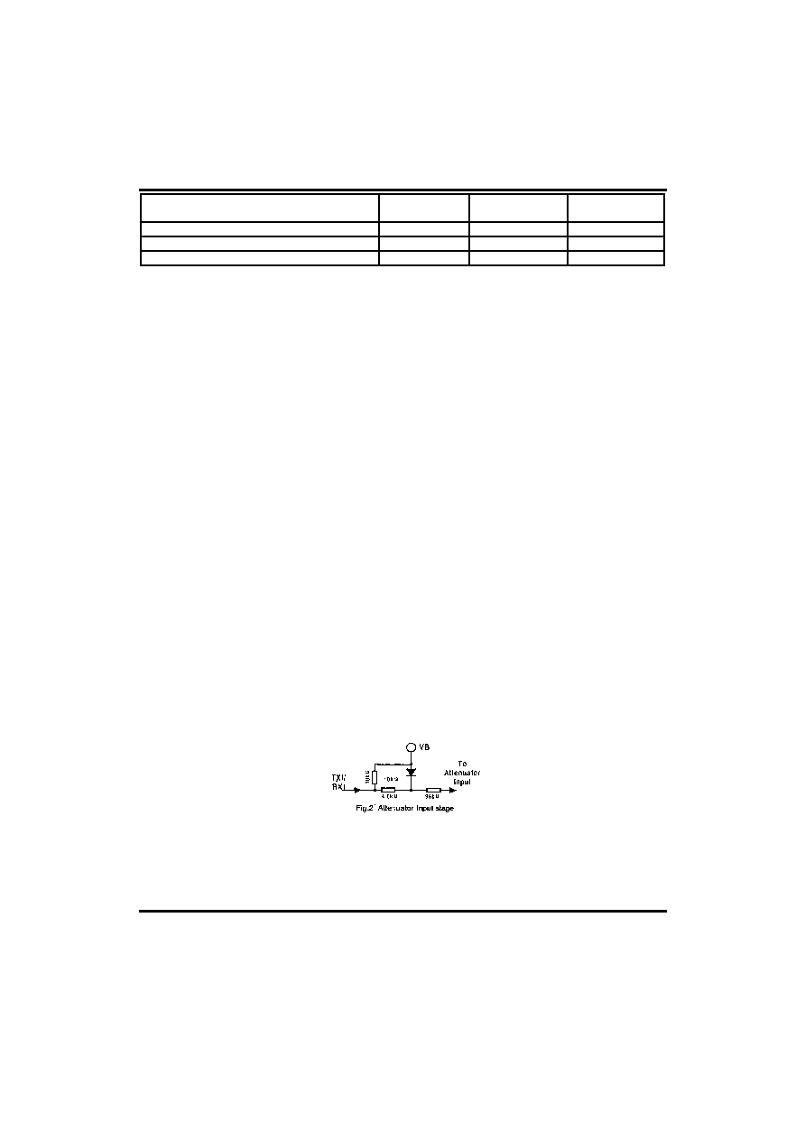
DIAL TONE DETECTOR
The dial tone detector is a comparator with one side connected to the receive input(RXI) and the other input
connected to VB with a 15mV offset( see Figure 4). If the circuit is in the receive mode, and the incoming signal is
greater than 15Mv(10 mVrms). The comparator's output will change, disabling the receive idle mode. The receive
attenuator will then be at a setting determined solely by the volume control.
The purpose of this circuit is to prevent the dial tone( which would be considered as continuous noise) from fading
away as the circuit would have the tendency to switch to the idle mode. By disabling the receive idle mode, the dial
tone remains at the normally expected full level.
AGC
The AGC circuit affects the circuit only in the receive mode, and only whenn the supply voltage( Vcc) is less than
3.5 volts. As Vcc falls below 3.5 volts., the transmit path attenuation changes such that the sum of the transmit and
receive gains remains constant. The purpose of this feature is to reduce the power) and current) used by the
speaker when a line-powered speakerphone is connected to a long line, where the available power is limited. By
reducing the speaker power, the voltage sag at Vcc is controlled, preventing possible erratic operation.
ATTENUATOR CONTROL BLOCK
The Attenuator control block has the seven inputs described below:
*The output of the comparator operated by RLO2 and TLO2( microphone/ speaker side), designated C1.
*The output of the comparator operated by RLO1 and TLO1( Tip/ Ring side), designated C2.
*The output of the transmit background noise monitor, designated C3.
*The output of the receive background noise monitor, designated C4.
* The volume control
* The dial tone detector
* The AGC circuit
The single output of the control block controls the two attenuators. The effect of C1~C4 is as follows:
UTC MC34118
LINEAR INTEGRATED CIRCUIT
UTC
UNISONIC TECHNOLOGIES CO., LTD.
10
QW-R108-007,A
INPUTS OUTPUT
MODE
C1 C2 C3 C4
Tx Tx 1 X
Transmit
Tx Rx Y Y
Fast
Idle
Rx Tx Y Y
Fast
Idle
Rx Rx X 1
Receive
Tx Tx 0 X
Slow
Idle
Tx Rx 0 0
Slow
Idle
Rx Tx 0 0
Slow
Idle
Rx Rx X 0
Slow
Idle
A definition of the above terms:
1. "Transmit" means the transmit attenuator is fully on( +6dB). And the receive attenuator is at max. attenuation
( -46dB).
2. "Receive" means both attenuators are controlled by the volume control. At max. volume the receive attenuator is
fully on( +6dB), and the transmit attenuator is at max.attenuation( -46dB).
3. "Fast Idle" means both transmit and receive speech are present in approximately equal levels. The attenuators
are quickly switched(30 ms) to idle until one speech level dominates the other.
4. "Slow Idle" means speech has ceased in both transmit and receive paths. The attenuators are then slowly
switched(1 second) to the idle mode.
5. Switching to the full transmit or receive from any other mode is at the fast rate(~30 ms).
A summary of the truth table is as follows:
1. The circuit will switch to transmit if: (A) both transmit level detectors sense signals relative to the respective
receive level detectors( TLI1 versus RLI1, TLI2 versus RLI2) and (B) the transmit background noise monitor
indicates the presence of speech.
2. The circuit will switch to receive if: (A) both receive level detectors sense higher signal levels relative to the
respective transmit level detectors and (B) the receive background noise monitor indicates the presence of speech.
3. The circuit will switch to the fast Idle mode if the level detectors disagree on the relative strengths of the signal
levels, and at least one of the background noise monitor indicates speech. For example, referring to the Figure 2, if
there is sufficient signal at the microphone amp. Output(TLI2) to over-ride the speaker signal(RLI2), and there is
sufficient signal at the receive input(RLI1) to over-ride the signal at the hybrid output(TLI1), and either or both
background noise monitors indicates speech, then the circuit will be in the fast idle mode. Two conditions which
can cause the fast idle mode to occur are : (A) when both talkers are attempting to gain control of the system by
talking at the same time. And (B) when one talker is in a very noisy environment, forcing the other to continually
over-ride that noise level. In general, the fast idle mode will occur infrequently.
4. The circuit will switch to the slow idle mode when: (A) both talkers are quiet( no speech present) or (B) when one
talker's speech level is continuously over-ride by noise at the other speaker's location. The time required to switch
the circuit between transmit, receive, fast idle, and slow idle is determined in part by the components at the CT
pin( pin14), (see the section on switching timers for a more complete explanation of the switching time components
A schematic of the CT circuitry is shown in Figure 5, and operates as follows:
*RT is typically 120k
, and CT is typically 5�F.
*To switch to the receive mode, I1 is turned on( I2 is off), charging the external capacitor to +240mV above VB( An
internal clamp prevents further charging of the capacitor).
*To switch to the transmit mode, I2 is turned on( I1 is off), bringing down the voltage on the capacitor to -240mV
with respect VB.
*To switch to idle quickly(fast idle), the current sources are turned off, and the internal 2k
resistor is switched in,
discharging the capacitor to VB with a time constant= 2k
x CT.
*To switch to idle slowly(slow idle), the current sources are turned off, the switch at the 2k
resistor is open, and the
capacitor discharges to VB through the external resistor RT with a time constant=RT x CT.

UTC MC34118
LINEAR INTEGRATED CIRCUIT
UTC
UNISONIC TECHNOLOGIES CO., LTD.
11
QW-R108-007,A
MICROPHONE AMPLIFIER
The microphone amplifier( Pins 10, 11) has the non-inverting input internally connected to VB while the inverting
input and the output are pinned out. Unlike most op-amps., the amplifier has an all-NPN output stage, which
maximizes phase margin and gain bandwidth. This feature ensures stability at gains less than unity, as wide range of
reactive loads. The open loop gain is typically 80Db(f<100Hz), and the gain bandwidth is typically 1MHz. The
maximum p-p output swing is typically 1 volt. less than Vcc with an output impedance of <10
until current limiting is
reached( typically 1.5mA). Input bias current at MCI is typically 40nA out of the pin. The muting function( Pin 12),
when activated, will reduce the gain of the amplifier to ~-39dB( with RMI=5.1k
) by shorting the range of ground and
Vcc. If the mute function is not used, the pin should be grounded.
HYBRID AMPLIFIER
The two hybrid amplifiers( at HTO+, HTO-, and HTI), in conjunction with an external transformer, provide the
two-to-four wire converter for interfacing to the telephone line. The gain of the first amplifier( HTI to HTO-) is set by
external resistors( gain = -RHF/RHI in Block Diagram), and its output drives the second amplifier, the gain of which is
internally set at -1. Unlike most op-amps., the amplifiers have an all- NPN output stage, which maximizes phase
margin and gain-bandwidth. This feature ensures stability at gains less than unity, as with a wide range of reactive
loads. The open loop gain of the first amplifier is typically 80dB, and the gain-bandwidth of each amplifier is ~1MHz.
The maximum p-p output swing is typically 1.2 volts. less than Vcc with an output impedance of <10
until current
limiting is reached( typically 8mA). The output current capability is guaranteed to be a minimum of 5mA. The bias
current at HTI is typically 30nA out of the pin. The connections to the coupling transformer are shown in the Block
Diagram. The block labeled ZBal is the balancing network necessary to match the line impedance.
FILTER
The operation of the filter circuit is determined by the external components. The circuit within the UTC MC34118,
from pins FI to FO is a butter with a high input impedance(>1M
), and a low output impedance(<50). The
configuration of the external components determines whether the circuit is a high-pass filter( as shown in Block
Diagram), a low-pass filter, or a band-pass filter. As a high-pass filter, with the components shown in Figure 6, the
filter will keep out 60Hz( and 120Hz) hum which can be picked up by the external telephone lines. As a low-pass
filter, with the components shown in Figure 7, it can be used to roll off the high end frequencies in the receive circuit,
which aids in protecting against acoustic feedback problems, with an appropriate choice of an input coupling
capacitor to the low-pass filter, a band pass filter is formed.

UTC MC34118
LINEAR INTEGRATED CIRCUIT
UTC
UNISONIC TECHNOLOGIES CO., LTD.
12
QW-R108-007,A
POWER SUPPLY, VB, and CHIP DISABLE
The power supply voltage at Vcc( Pin 4) is to be between 3.5 and 6.5 volts. for normal operation, with reduced
operation possible down to 2.8 volts. The output voltage at VB( Pin 15) is ~(Vcc-0.7)/2, and provides the AC ground
for the system. The output impedance at VB is ~400
and in conjunction with the external capacitor at VB, forms a
low pass filter for power supply rejection. The choice of capacitor is application dependent based on whether the
circuit is powered by the telephone line or power supply. Since VB biases the microphone and hybrid amplifiers, the
amount of supply rejection at their outputs is directly related to the rejection at VB, as well as their respective gains.
The Chip Disable(Pin 3) permits powering down the IC to conserve power and/or for muting purposes. With CD<0.8
volts., normal operation is in effect. With CD>2 volts. and <Vcc, the IC is powered down. In the powered down mode,
the microphone and the hybrid amplifiers are disabled, and their outputs go to a high impedance state. Additionally,
the bias is removed from the level detectors. The bias is not removed from the filter( Pin 1, 2), the attenuators( Pin 8,
9, 21, 22), or from Pins 13, 14, and 15( the attenuators are disabled, however, and will not pass a signal impedance
at CD is typically 90k
, has a threshold of ~1.5 volts., and the voltage at this pin must be kept within the range of
ground and Vcc). If CD is not used, the pin should be grounded.
UTC MC34118
LINEAR INTEGRATED CIRCUIT
UTC
UNISONIC TECHNOLOGIES CO., LTD.
13
QW-R108-007,A
APPLICATION CIRCUIT