
T-1 PACKAGE
PIN PHOTODIODE
MID-30A12
Description
Package Dimensions
The MID-30A12 is a PIN photodiode mou-
nted in a lensed , special dark plastic package.The lens-
ing effect of the package allows an acceptance half view
angle of 10° that is measured from the optical axis to the
half power point .
Features
l
High photo sensitivity
l
Low junction capacitance
l
Hight cut-off frequency
l
Fast switching time
l
Good spectral matching IRED (
p=940nm) type.
Absolute Maximum Ratings
@ T
A
=25
o
C
Parameter
Maximum Rating
Unit
Power Dissipation
100
mW
Reverse Break Down Voltage
30
V
Operating Temperature Range
Storage Temperature Range
Lead Soldering Temperature
02/04/2002
-55
o
C to +100
o
C
-55
o
C to +100
o
C
260
o
C for 5 seconds
Notes :
1. Tolerance is ± 0.25 mm (.010") unless otherwise noted.
2. Protruded resin under flange is 0.8 mm (.031") max.
3. Lead spacing is measured where the leads emerge from the package.
Unit : mm (inches )
Unity Opto Technology Co., Ltd.
2.54 NOM.
(.100)
C
A
0.50 TYP.
(.020)
1.00
(.040)
SEE NOTE 2
3.00
(.118)
1.00MIN.
(.040)
23.40MIN.
(.920)
5.25
(.207)
0.80±0.50
(.031)
FLAT DENOTES CATHODE
4.00
(.157)
SEE NOTE 3
MID-30A12
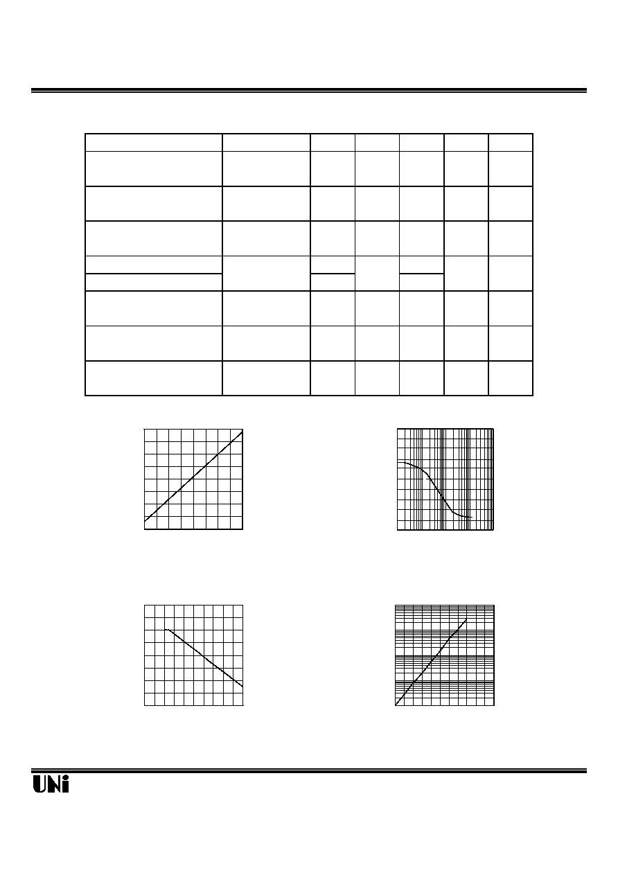
Optical-Electrical Characteristics
@ T
A
=25
o
C
Parameter
Test Conditions
Symbol
Min.
Typ.
Max.
Unit
Reverse Break Down Voltage
I
R
=100
µ
A
Ee=0
Reverse Dark Current
V
R
=10V
Ee=0
Open Circuit Voltage
=940nm
Ee=0.1mW/cm
2
Rise Time
V
R
=10V
=940nm
Tr
40
nsec
Fall Time
R
L
=1K
Tf
30
Light Current
V
R
=5V,
=940nm
Ee=0.1mW/cm
2
Total Capacitance
V
R
=3V, f=1MH
Z
Ee=0
Half Acceptance Angle
V
R
=5V
Ee=0.1mW/cm
2
Typical Optical-Electrical Characteristic Curves
02/04/2002
V
(BR)R
30
V
I
D
30
nA
V
OC
350
mV
I
L
1
4
µ
A
C
T
15
pF
deg.
2
1/2
25
Unity Opto Technology Co., Ltd.
Total Power Dissipation
mW
0
50
100
150
200
0
20
40
60
80 100
Ambient Temperature -
o
C
FIG.3 TOTAL POWER DISSIPATION
VS. AMBIENT TEMPERATURE
0.1
1
10
100
1000
0
20 40 60 80 100
Ambient Temperature -
o
C
FIG.4 DARK CURRENT VS AMBIENT TEMPERATURE
V
R
=10, Ee=0 mw/cm
2
Capacitance C - pF
Reverse Voltage- V
R
FIG.2 CAPACITANCE VS. REVERSE
VOLTAGE
F=1MHZ ; Ee=0mW/cm
2
0
20
40
60
80
100
0.01 0.1 1 10 100
0
1000
2000
3000
4000
0
5
10
15
20
Reverse Voltage -
o
C
FIG.1 DARK CURRENT VS REVERSE VOLTAGE
TAMB=25
o
C, Ee=0 mW/cm
2
Dark Current I
R
- pA
Dark Current I
R
- nA
MID-30A12
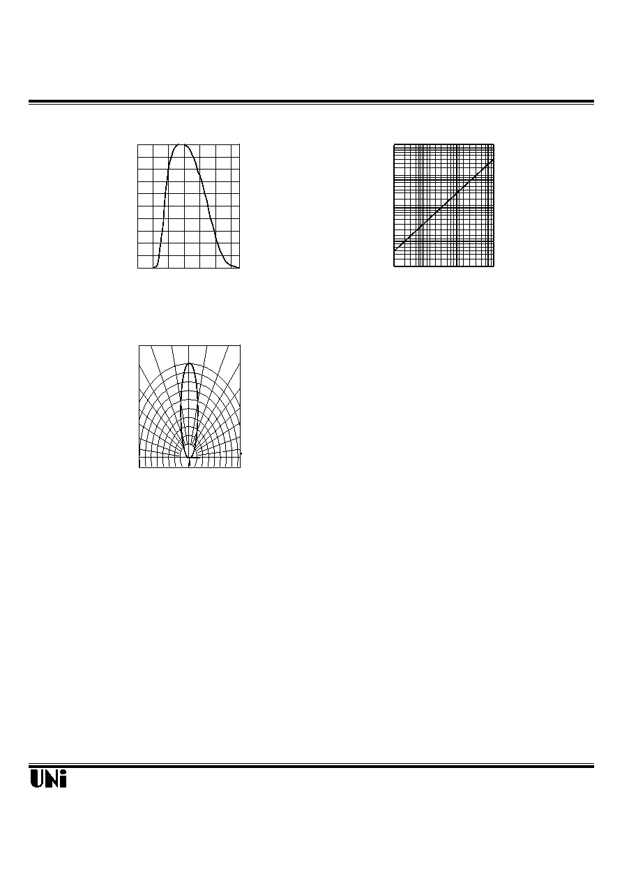
Typical Optical-Electrical Characteristic Curves
02/04/2002
Unity Opto Technology Co., Ltd.
Wavelength (nm)
FIG.5 RELATIVE SPECTRAL SENSITIVITY
VS. WAVELENGTH
0.01 0. 1 1 10
Irradiance Ee (mW/cm
2
)
FIG.6 PHOTOCURRENT VS.
IRRADIANCE = 950 nm
Photocurrnet Ip -
µ
A
0.1
1
10
100
1000
0.5 0.3 0.1 0.2 0.4 0.6
1.0
0.9
0.8
0° 10° 20°
FIG.7 SENSITIVITY DIAGRAM
30°
40°
50°
60°
70°
80°
90°
Relative Response
0
20
40
60
80
100
700 800 900 1000 1100 1200