2
For further information please visit
www.triquint.com
Datasheet rev 6.0; December 16, 2004.
TQL5000
DATASHEET
WLAN PRODUCTS
Package Pin-out:
LNA for 5GHz UNII Band
802.11a Systems
Features
4.9 to 5.9 GHz Frequency Coverage
Low Noise Figure
High Gain
Low Current: 8mA Typical @ 3V
50-ohm Input and Output Match
GaAs pHEMT Technology
Leadless 1.3 x 2.0 x 0.4 mm Lead
Free SMT Package
Applications
802.11a WLAN
PCs and Mobile Devices
WLAN Access Points
WLAN Repeaters
Product Description:
The TQL5000 is a low noise amplifier designed for 802.11a receive applications
for the WLAN market. The device exhibits industry-leading noise figure and
power consumption while maintaining high intercept performance. It requires a
single 3 V supply voltage and draws 8 mA. The LNA is manufactured using
TriQuint's GaAs pHEMT process and is packaged in an ultra-small, low-profile
1.3mm x 2mm x 0.4mm Lead Free SLIM-7 package.
Selected Electrical Specifications:
Parameter min
typ
Max
units
Frequency
Range
4900 - 5900
MHz
Noise Figure (with onchip match)
1.3
dB
Small Signal Gain
16.5
18
dB
Input Power (IP1dB)
-13
dBm
Input IP3
-3
dBm
Test Conditions: Ta=25°C; Vdd=3.0V
RF
Input
RF
Output
Vdd
Src

TQL5000
Datasheet
Absolute Maximum Ratings
Parameter
Symbol
Value
Unit
min
max
Supply Voltage Range
Vddl
0
6
V
DC Voltage, @ RF Ports
Vrf
-0.3
0.3
V
DC Volgate, @ GND ports
Vgnd
-0.3
0.3
V
Operating Temperature Range
Ta
-40
85
°C
Channel Temperature
Tch
150
°C
Storage Temperature Range
Tstg
-55
150
°C
Power Dissipation
Pdiss
0.2
W
Maximum Input Power
P
I
0
dBm
General Electrical Characteristics
1,2
LNA Performance:
Parameter min
typ
max
units
Frequency
Range
4900 - 5900
MHz
Small Signal Gain
16.5
18
dB
Gain Variation vs Vdd
0.5
dB
Gain Variation vs Frequency
1.5
dB
Noise Figure (with on-chip matching)
1.3
dB
Input Power (IP1dB)
-13
dBm
Input
IP3
-3
dBm
Isolation
30
dB
Stability
10:1
Harmonics (2
nd
, 3
rd
, 4
th
)
-30
dBc
Input VSWR (with on-chip matching)
1.7
Output VSWR (with on-chip matching)
2
Electrical Characteristics
Parameter min
typ
max
Unit
Vdd Supply Voltage
2.7
3.0
3.6
V
Supply Current: Vdd = 3.0V
8
mA
1
Test Conditions: Ta=25oC, unless otherwise noted,
2
AC performance is guaranteed at 25 Deg-C,

TQL5000
Datasheet
Applications Information
0.4 Max
1
3
2
6
5
4
1.3
+0.1 / -0.05
2.
+0.1 / -0.05
0.4 Max
Bottom View
1.3
+0.1 / -0.05
2.
+0.1 / -0.05
1.3
+0.1 / -0.05
2.
+0.1 / -0.05
2.
1.3mm x 2mm SLIM-7 Package
Top View
+0.1 / -0.05
4
5
6
2
3
1
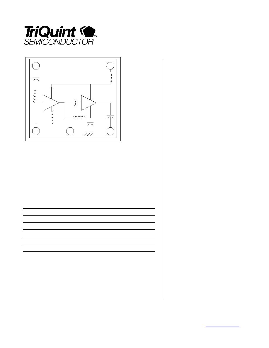
Functional Block Diagram:
RF
Input
RF
Output
Vdd
Src
Pin Assignments:
PIN
Symbol
Abbreviation
Description
1
Vdd
Vdd
Drain Supply Voltage
2
Ground
GND
RF and DC Ground
3
RF IN
RF IN
RF Input
4
SRC
SRC
Source Grounding
5
N/C
N/C
No Connection
6
RF OUT
RF OUT
RF Output
Application Circuit:
LNA_OUT
VDD
LNA_IN
P ort
P 2
Num =2
R
R1
R=5.1 Ohm
C
C2
C=10 nF
P ort
P 3
Num =3
TS LP 7_cs
X3
TQL5000
6
5
4
3
2
1
P ort
P 1
Num =1
4
For further information please visit
www.triquint.com
Datasheet rev 6.0; December 16, 2004.

TQL5000
Datasheet
TQL5000 5GHz LNA; TQL5000- V1.0 Evaluation board
Bill of Materials
Layer/Descriptions
Dielectric: FR4: Er=4.6
Top: 1 oz. Plated Copper
Dielectric 1 : 8 mils
Mid 1: 1 oz. Copper
Dielectric 2: 28 mils
Mid 2: 1 oz. Copper
Dielectric 3: 6 mils
Bottom: 1 oz. Plated Copper
TQL5000
Datasheet
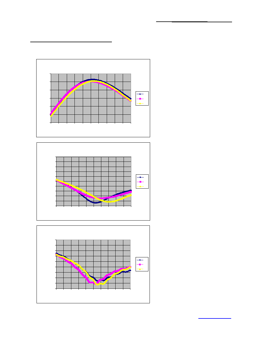
TQL5000 Measured Performance:
TriQuint TQL5000- V1.0 Evaluation Board
Measurement Conditions Ta = 25
°
C, Vdd=3.0, Idd=8.2mA
TQL5000 Rev 2 Gain
14
15
16
17
18
19
20
4.5
4.7
4.9
5.1
5.3
5.5
5.7
5.9
6.1
6.3
6.5
Fre q (GHz)
S2
1
(
d
B
)
#1
#2
#3
TQL5000 Rev 2 Input Matching
-20.00
-18.00
-16.00
-14.00
-12.00
-10.00
-08.00
-06.00
-04.00
-02.00
00.00
4.5
4.7
4.9
5.1
5.3
5.5
5.7
5.9
6.1
6.3
6.5
Fre q (GHz)
S2
1
(
d
B
)
#1
#2
#3
S
1
1
(d
B)
TQL5000 Rev 2 Output Matching
-18.00
-16.00
-14.00
-12.00
-10.00
-08.00
-06.00
-04.00
-02.00
00.00
4.5
4.7
4.9
5.1
5.3
5.5
5.7
5.9
6.1
6.3
6.5
Fre q (GHz)
S
2
1
(
d
B
)
#1
#2
#3
S
2
2
(d
B
)
6
For further information please visit
www.triquint.com
Datasheet rev 6.0; December 16, 2004.
TQL5000
Datasheet
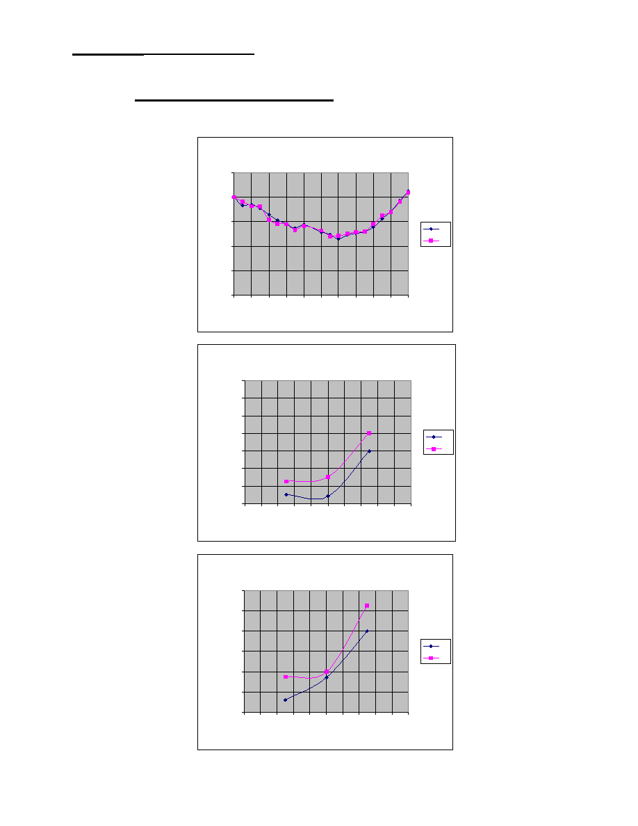
TQL5000 Measured Performance:
TriQuint TQL5000- V1.0 Evaluation Board
Measurement Conditions Ta = 25
°
C, Vdd=3.0, Idd=8.2mA
TQL5000 Rev 2 NF
1
1.1
1.2
1.3
1.4
1.5
4.5 4.7 4.9 5.1 5.3 5.5 5.7 5.9 6.1 6.3 6.5
Freq (Ghz)
NF (dB)
#1
#2
TQL5000 Rev 2 IIP3
-07.00
-06.00
-
-
-
-
IIP3 (dBm)
05.00
04.00
03.00
02.00
-01.00
00.00
4.5 4.7 4.9 5.1 5.3 5.5 5.7 5.9 6.1 6.3 6.5
Freq (Ghz)
#1
#2
TQL5000 Rev 2 IP1dB
-16.00
-
-
-
-
IIP
3
(dBm
)
15.50
15.00
14.50
14.00
-13.50
-13.00
4.5 4.7 4.9 5.1 5.3 5.5 5.7 5.9 6.1 6.3 6.5
Freq (Ghz)
#1
#2

TQL5000
Datasheet
8
For further information please visit
www.triquint.com
Datasheet rev 6.0; December 16, 2004.
Package Outline SLIM7

TQL5000
Datasheet
Package Marking
XXXX
Line 1: XXXX last 4 digits of TQS lot number
Pin 1
Caution: Electrostatic discharge sensitive. Observe handling Precautions!
Ordering Information
Type
Marking
Ordering code
(tape and reel)
Package
TQL5000
XXXX
TBD
SLIM-7
Additional Information
For latest specifications, additional product information, worldwide sales and distribution locations, and information about TriQuint:
Web: www.triquint.com
Tel: (503) 615-9000
Email:
info_wireless@tqs.com
Fax: (503) 615-8902
For technical questions and additional information on specific applications:
Email:
info_wireless@tqs.com
The information provided herein is believed to be reliable; TriQuint assumes no liability for inaccuracies or omissions. TriQuint assumes no responsibility for the use of
this information, and all such information shall be entirely at the user's own risk. Prices and specifications are subject to change without notice. No patent rights or
licenses to any of the circuits described herein are implied or granted to any third party.
TriQuint does not authorize or warrant any TriQuint product for use in life-support devices and/or systems.
Copyright © 2003 TriQuint Semiconductor, Inc. All rights reserved.
Revision 1.2 , August 5, 2003
For additional information and latest specifications, see our website: www.triquint.com
9