Äîêóìåíòàöèÿ è îïèñàíèÿ www.docs.chipfind.ru
WIRELESS COMMUNICATIONS DIVISION
For additional information and latest specifications, see our website: www.triquint.com
1
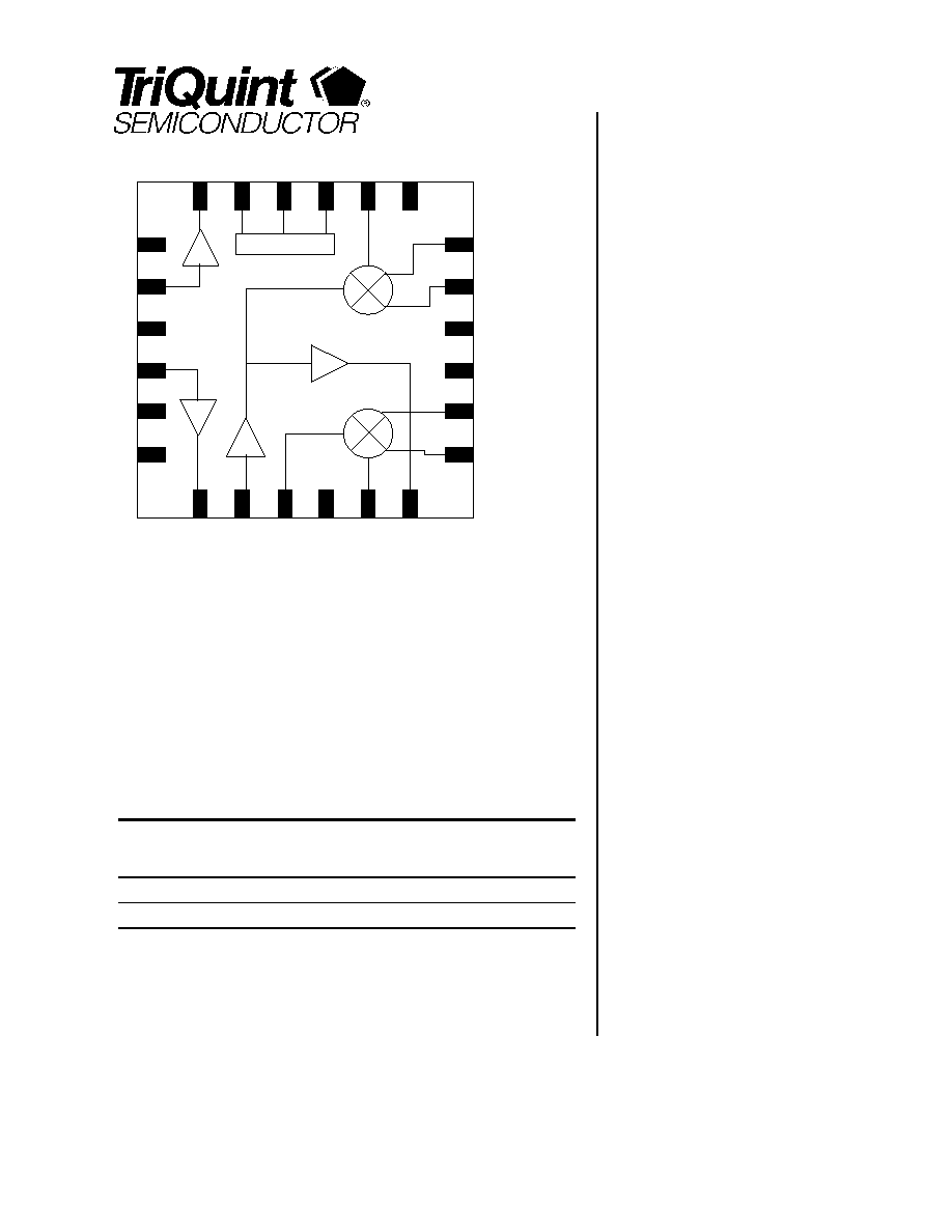
Package Pin-out:
Product Description:
The TQ5638 is a CDMA Rx Receiver designed for KPCS-Band, Dual-Mode operation.
The device supports KPCS CDMA and GPS. The IF range is from 80 MHz to 230MHz
with external tuning. The Low Noise Amplifiers have an adjustable third order intercept
(IP3) to minimize inter-modulation and cross-modulation effects. The mixers are
designed for differential IF outputs (single-ended or differential IF for GPS modes),
and
they feature excellent linearity and low noise figure.
This device is available in a 4X4 mm MLF package with 24 pins. The TQ5638 front-
end receiver is capable of meeting all electrical requirements in accordance with the
TIA/EIA 98-C Wireless Communication standard.
Selected Cascade Electrical Specifications:
Operating Mode (Cascade)
Cascade
Gain
(dB)
Cascade
NF
(dB)
Cascade
IP3
(dBm)
Current
(mA)
PCS-Band, High-Gain, High Linearity
26
2.2
-2.0
28
A-GPS
37
1.7
-17.5
19
Note 1:
Test Conditions CDMA Mode: V
CC
=2.75VDC, Tc=25°C, IS-95/98 Modulation, Data includes the
following image reject filters (PCS SAWTEK P/N 856080, GPS SAWTEK P/N 856135)
TQ5638
PRELIMINARY DATA SHEET
2.8V SiGe Dual-Mode CDMA
Rx Receiver
Features
KPCS-CDMA and GPS operation
Excellent Cross Modulation Performance
Low current consumption
9.0 dBm PCS LNA IIP3
11.0 dBm PCS Mixer IIP3
Excellent Noise and Gain performance
Adjustable third order intercept on LNA
stage
Flexible IF frequency range from 80 230
MHz
TX LO Buffer included
Small 4x4 Package
Full ESD Protection
Few external components
System Advantage
Most compact integrated receiver for KPCS
CDMA and A-GPS applications
IS-98 IMD requirements met with 2 gain
states simplifying calibration procedures
High mixer linearity eliminates potential call
drop issues associated with gain switching
Enhanced PCS linearity enables use of
FBAR or SAW PCS duplexers
Best I in class A-GPS cascade gain for
maximum takeover
Applications
KPCS band/A-GPS CDMA (IS-95/98) based
mobile phones
`
Iset
PLNA_IN
VDD_LNA
GLNA_IN
GPS_GND
VDD_LO
GL
NA
_
O
UT
PLO_IN
GLO_IN
GM
IX_IN
PLO_OUT
GM_OUT-
GM_OUT+
Vdd_MIX
MIX_GND
PM_OUT-
PM_OUT+
V
DD_
DIG
PM
IX_IN
BUFFEN
LIN/GPS
PC
S_ON
P
L
NA
_
O
UT
Logic Control
TQ5638
GND
TQ5638-Preliminary
Data Sheet
2
For additional information and latest specifications, see our website: www.triquint.com
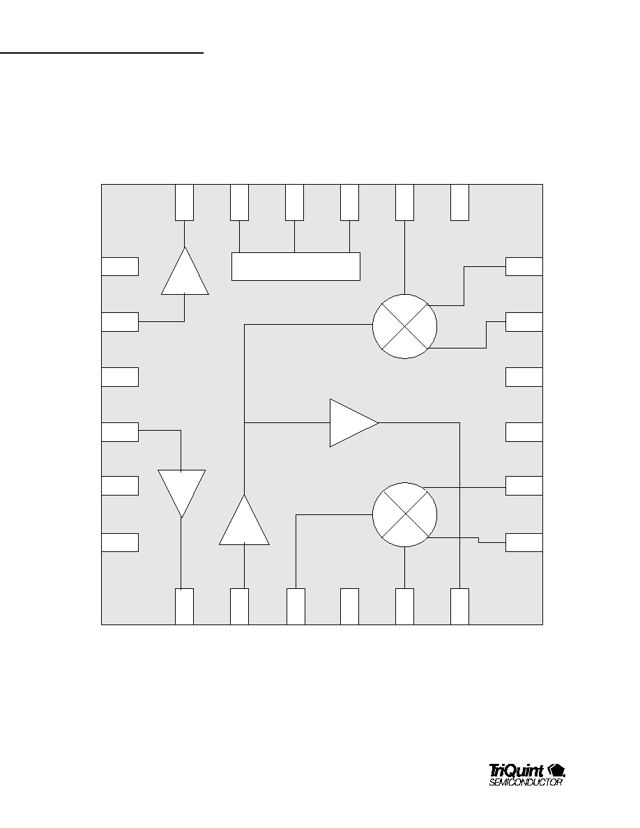
`
Iset
PLNA_IN
VDD_LNA
GLNA_IN
GPS_GND
VDD_LO
GLNA_OUT
PLO_IN
GLO_IN
GMIX_IN
PLO_OUT
GM_OUT-
GM_OUT+
Vdd_MIX
MIX_GND
PM_OUT-
PM_OUT+
VDD_DIG
PMIX_IN
BUFFEN
LN/GPS
PCS_ON
PLNA_OUT
Logic Control
TQ5638
GND
Preliminary TQ5638
Data Sheet
For additional information and latest specifications, see our website: www.triquint.com
3
Pin Descriptions:
Pin Name
Pin #
Description and Usage
Iset_PCS
1 Bias resistor for PCS LNA.
PLNA_IN
2 PCS LNA input. Requires a blocking capacitor, which may be used as part of the
input-matching network.
Vdd_LNA
3 Power supply pin for PCS and GPS LNAs. Bypass with a capacitor as close to the
pin as possible.
GLNA_IN
4 GPS LNA input. Requires LC match.
GPS_GND
5 GPS Ground.
Vdd_LO
6 Supply voltage for LO buffers.
GPS_LNA_OUT
7 GPS LNA output.
PLO_IN
8 PCS LO input.
GLO_IN
9 GPS LO input.
GND
10 Ground.
GPS_Mix_IN
11 GPS Mixer input.
PLO_OUT
12 PCS LO buffer output. Does not require a blocking capacitor.
GPS_Mix_OUT-
13 Negative GPS IF output.
GPS_Mix_OUT+
14 Positive GPS IF output.
Vcc_Mix
15 Supply voltage for all mixers.
MIX_GND
16 Mixer Ground.
PCDMA_OUT-
17 Negative CDMA output.
PCDMA_OUT+
18 Positive CDMA output.
Vdd_DIG
19 Supply voltage for Logic Control Circuits.
PM_IN
20 PCS Mixer RF input.
BUFFEN
21 LO output buffer enable. Set BUFFEN pin HIGH to power up the PCS LO buffer
output.
LIN/GPS
22 Logic input for high or low linearity. Logic HIGH selects High Linearity.
PCS_ON
23 Power on for PCS. Logic HIGH selects PCS Band.
PLNA_OUT
24 PCS LNA output. Requires a pull-up inductor to Vcc and a series blocking capacitor,
which can be used as part of the output-matching network.
TQ5638-Preliminary
Data Sheet
4
For additional information and latest specifications, see our website: www.triquint.com
Absolute Maximum Ratings
Symbol
Parameter
Absolute Maximum
Value
Units
V
CC
_LNA
,
V
CC_
LO_Tx
,
V
CC
_MIX, V
CC
_DIG
Power Supply Voltage
-0.5 to 4.0
VDC
PCS_ON, LIN/GPS, BUFFEN
Logic Control Lines
-0.5 to 4.0
VDC
I
CC
_LNA
,
I
CC
_LO_Tx
,
I
CC
_MIX, I
CC
_DIG
Supply Currents
50
mA
PLO_IN, GLO_IN
LO Input Levels
+5.0
dBm
PLNA_IN, GPS_LNA_IN
LNA Input
+5.0
dBm
I
SET
_PCS
LNA IP3 Adjustment Input
1
mA
T
C
Case Temperature, Survival
-40 to +100
°C
T
STG
Storage Temperature
-40 to +150
°C
Note: The part may not survive all maximums applied simultaneously.
General Electrical Characteristics
1,2,3
Parameter
Conditions
Min.
Typ/Nom
Max.
Units
PCS Band
1840
1855
1870
MHz
A-GPS Band
1575.42
MHz
Low
1620
1650
MHz
KPCS Band, IF=220.38MHz
High
2060
2090
MHz
Low
1355.04
MHz
LO Frequency Range
GPS Band, IF=220.38MHz
High
1795.80
MHz
IF Range
PCS, and GPS Bands
80
220.38
230
MHz
LO Input Power Level
PCS, and GPS Bands
-10
-5
0
dBm
LO Tx Buffer Output Power Level
PCS Band
-8
-3
dBm
Note 1: Test Conditions: V
CC
=2.75VDC, T
C
= 25
°
C unless otherwise specified.
Note 2: Min./Max. limits are at +25
°
C case temperature unless otherwise specified.
Note 3: TriQuint Test Board.
Preliminary TQ5638
Data Sheet
For additional information and latest specifications, see our website: www.triquint.com
5
Cascade RF Electrical Characteristics (PCS Band, CDMA Modulation)
1,2
Parameter
Conditions
Min.
Typ/Nom
Max.
Units
High Gain, High-Linearity Mode
BAND_SEL = Low, Gain = High, LIN/GPS = High
Cascade Conversion Gain
26.3
dB
Cascade Noise Figure
2.2
dB
Cascade Input IP3
-2
dBm
Supply Current
28
mA
High Gain, Low-Linearity Mode
BAND_SEL = Low, Gain = High, LIN/GPS = Low
Cascade Conversion Gain
25.3
dB
Cascade Noise Figure
2.3
dB
Cascade Input IP3
-5.5
dBm
Supply Current
20.5
mA
Note 1: Test conditions (devices screened for Conversion Gain, Noise Figure and IIP3 to the above limits): Vcc=2.75V, RF=1855MHz, LO=1635MHz, IF=220MHz, LO
input = -5.0dBm, RF input = -35dBm (High Gain Mode), unless otherwise specified. TriQuint Test Board. Data includes image reject filter (SAWTEK P/N 856080), Note
2:
Min./Max. limits are at +25
°
C case temperature unless otherwise specified.
Cascade RF Electrical Characteristics (GPS Band)
1,2
Parameter
Conditions
Min.
Typ/Nom
Max.
Units
GPS Mode
BAND_SEL = Low, Gain = Low, LIN/GPS =
High
Cascade Conversion Gain
37.0
dB
Cascade Noise Figure
1.7
dB
Cascade Input IP3
-17.5
dBm
Supply Current
18.5
mA
Note 1: Test conditions (devices screened for Conversion Gain, Noise Figure and IIP3 to the above limits): Vcc=2.75V, RF=1575.42MHz, LO=1355.04MHz,
IF=220.38MHz, LO input = -5.0dBm, RF input = -50dBm. TriQuint Test Board. Data includes image reject filter (SAWTEK P/N 856135)
Note 2:
Min./Max. limits are at +25
°
C case temperature unless otherwise specified.
DC Supply Electrical Characteristics (All-Modes)
1,2
Parameter
Conditions
Min.
Typ/Nom
Max.
Units
Supply Voltage
2.7
2.75
3.3
V
Control Voltage High
1.7
V
Control Voltage Low
0.5
V
LO Rx Buffer Supply Current
7
mA
LO Tx Buffer Current
BUFFEN=High
6
mA
Logic Current
Low, High
-5
100
µA
Power Down Supply Current
PCS_ON= Low, LIN/GPS = Low
10
µA