
WIRELESS COMMUNICATIONS DIVISION
For additional information and latest specifications, see our website: www.triquint.com
1
LO IN
1
2
3
4
6
7
9
10
11
12
13
14
15
16
GND
GND
GND
Vdd MXR
5
VDD LNA
RF IN
Sleep
Control
IF OUT/Vdd
8
GND
GND
GND
GND
GND
LNA Out
MXR RF IN
TQ5622
DATA SHEET
3V PCS Receiver IC
With Power- Down
Features
Power-Down, "Sleep" Mode
Single 2.8V operation
Low-current operation
Small QSOP-16 plastic package
Few external components
Applications
PCS, IS-136 based TDMA Mobile
Phones
Product Description
The TQ5622 is a 3V, RF receiver IC designed specifically for PCS band TDMA
applications. It's RF performance meets the requirements for products designed to the
IS-136 TDMA standards. The TQ5622 includes a power�down mode which allows
current saving during standby and the non-operating portion of the TDMA pulse. The
TQ5622 contains LNA and Mixer circuits matched to the 1900MHz PCS band.
The mixer uses a high-side LO frequency. The IF has a usable frequency range of 85
to 150MHz. The LNA Output and Mixer Input ports are internally matched to simplify
the design and keep the number of external components to a minimum. The TQ5622
achieves excellent RF performance with low current consumption which gives long
standby times in portable applications. The small QSOP-16 package is ideally suited
for PCS band mobile phones.
Electrical Specifications
1
Parameter
Min
Typ
Max
Units
Frequency
1930
1990
MHz
Gain
17.5
dB
Noise Figure
2.8
dB
Input 3
rd
Order Intercept
-9
dBm
DC supply Current
12.0
mA
Note 1: Test Conditions: Vdd=2.8VDC, Tc=25�C, Filter IL=2.5dB, RF=1960MHz, LO=2095MHz,
IF=135MHz, LO input=-7dBm

TQ5622
Data Sheet
2
For additional information and latest specifications, see our website: www.triquint.com
Electrical Characteristics
1,2
Parameter
Conditions
Min.
Typ/Nom
Max.
Units
RF Frequency
1930
1990
MHz
LO Frequency
2015
2140
MHz
IF Frequency
85
150
MHz
LO input level
-7
-4
0
dBm
Supply voltage
2.7
2.8
4.0
V
Gain
16.0
17.5
dB
Gain Variation vs. Temp.
-40 to 85 �C
+/-2.0
dB
Noise Figure
2.8
3.5
dB
Input 3
rd
Order Intercept
-11.0
-9
dBm
Return Loss
LNA input � with external match
LNA output
Mixer RF input, externally matched
Mixer LO input
10
10
10
10
dB
dB
dB
dB
Isolation
LO to LNA RF in
LO to IF; after external IF match
RF to IF; after external IF match
35
40
20
dB
dB
dB
IF Output Impedance
Vdd = 2.8V; Sleep mode, Device On
Vdd = 2.8V; Sleep mode, Device Off
Vdd = 0V
500
Approx. Open
<50
Ohm
Ohm
Ohm
Power Down, "sleep"
Device On Voltage
Device Off Voltage
0
Vdd
0
Vdd
VDC
VDC
Supply Current, Sleep mode, Device On
Tc = + 25 �C
12
15
mA
Supply Current, Sleep mode, Device Off
Enable voltage = 0, LO Drive off
100
1000
�A
Operating Temperature, case
-40
25
+85
�C
Note 1: Test Conditions: Vdd=2.8VDC, Filter IL=2.5dB, RF=1960MHz, LO=2095MHz, IF=135MHz, LO input=-7dBm, T
C
= 25
�C, unless otherwise specified.
Note 2: Min./Max. limits are at +25
�C case temperature unless otherwise specified.
Absolute Maximum Ratings
Parameter
Value
Units
DC Power Supply
5.0
V
Power Dissipation
500
mW
Operating Temperature
-55 to 100
�C
Storage Temperature
-60 to 150
�C
Signal level on inputs/outputs
+20
dBm
Voltage to any non supply pin
-0.3 to Vdd + 0.3
V
TQ5622
Data Sheet
For additional information and latest specifications, see our website: www.triquint.com
3
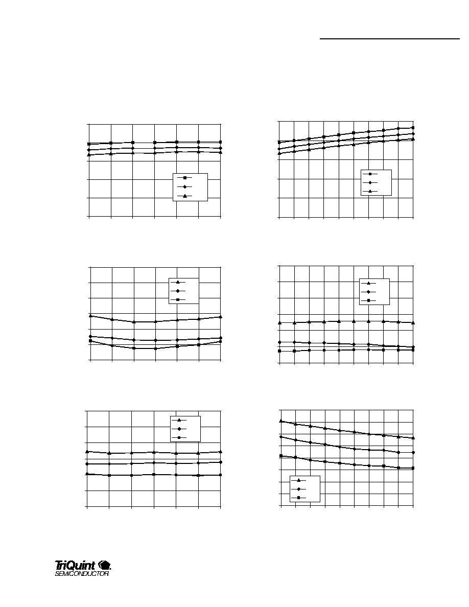
Typical Performance
Test Conditions (Unless Otherwise Specified): Vdd=2.8VDC, Tc=25�C, filter IL=2.5dB, RF=1960MHz, LO=2095MHz, IF=135MHz, LO input=-7dBm
Gain vs. Frequency vs. Temperature
0
5
10
15
20
25
1930
1940
1950
1960
1970
1980
1990
Frequency (MHz)
G
a
in
(d
B
)
-40C
+25C
+85C
Input IP3 vs. Frequency vs. Temperature
-12
-10
-8
-6
-4
-2
0
1930
1940
1950
1960
1970
1980
1990
Frequency (MHz)
I
nput
I
P
3 (
d
Bm)
+85C
+25C
-40C
NF vs. Frequency vs. Temperature
0
1
2
3
4
5
6
1930
1940
1950
1960
1970
1980
1990
Frequency (MHz)
NF (
d
B)
+85C
+25C
-40C
Gain vs. Vdd vs. Temperature
0
5
10
15
20
25
2.7
2.8
2.9
3
3.1
3.2
3.3
3.4
3.5
3.6
Vdd (volts)
G
a
in
(d
B
)
-40C
+25C
+85C
Input IP3 vs Vdd vs Temperature
-12
-10
-8
-6
-4
-2
0
2.7
2.8
2.9
3
3.1
3.2
3.3
3.4
3.5
3.6
Vdd (volts)
I
nput
I
P
3 (
d
Bm)
+85C
+25C
-40C
NF vs. Vdd vs. Temperature
0
0.5
1
1.5
2
2.5
3
3.5
4
2.7
2.8
2.9
3
3.1
3.2
3.3
3.4
3.5
3.6
Vdd (volts)
NF (
d
B)
+85C
+25C
-40C

TQ5622
Data Sheet
4
For additional information and latest specifications, see our website: www.triquint.com
Application/Test Circuit
L3
F1900
IF out
V IF
LNA in
LO in
V LNA
V MX
L1
R2
R1
L3
C6
C4
C5
1
2
3
4
5
6
7
8
16
15
14
13
12
11
10
9
R3
C2
C3
L4
Sleep Mode
C7
Bill of Material for TQ5622 Receiver Application/Test Circuit*
Component
Reference Designator
Part Number
Value
Size
Manufacturer
Receiver IC
U1
TQ5622
QSOP-16
TriQuint Semiconductor
Capacitor
C1
Not used
Capacitor
C2
5.6pF
0603
Capacitor
C3,C6
1000pF
0603
Capacitor
C4
10pF
0603
Capacitor
C5
15pF
0603
Capacitor
C7
1.0pF
0402
Inductor
L1
2.2nH
0603
Inductor
L2
150nH
0805
Inductor
L3
2.7nH
0603
Inductor
L4
3.9nH
0402
Filter
F1
1930-1990MHz
Toyocom
* May vary due to printed circuit board layout and material.

TQ5622
Data Sheet
For additional information and latest specifications, see our website: www.triquint.com
5
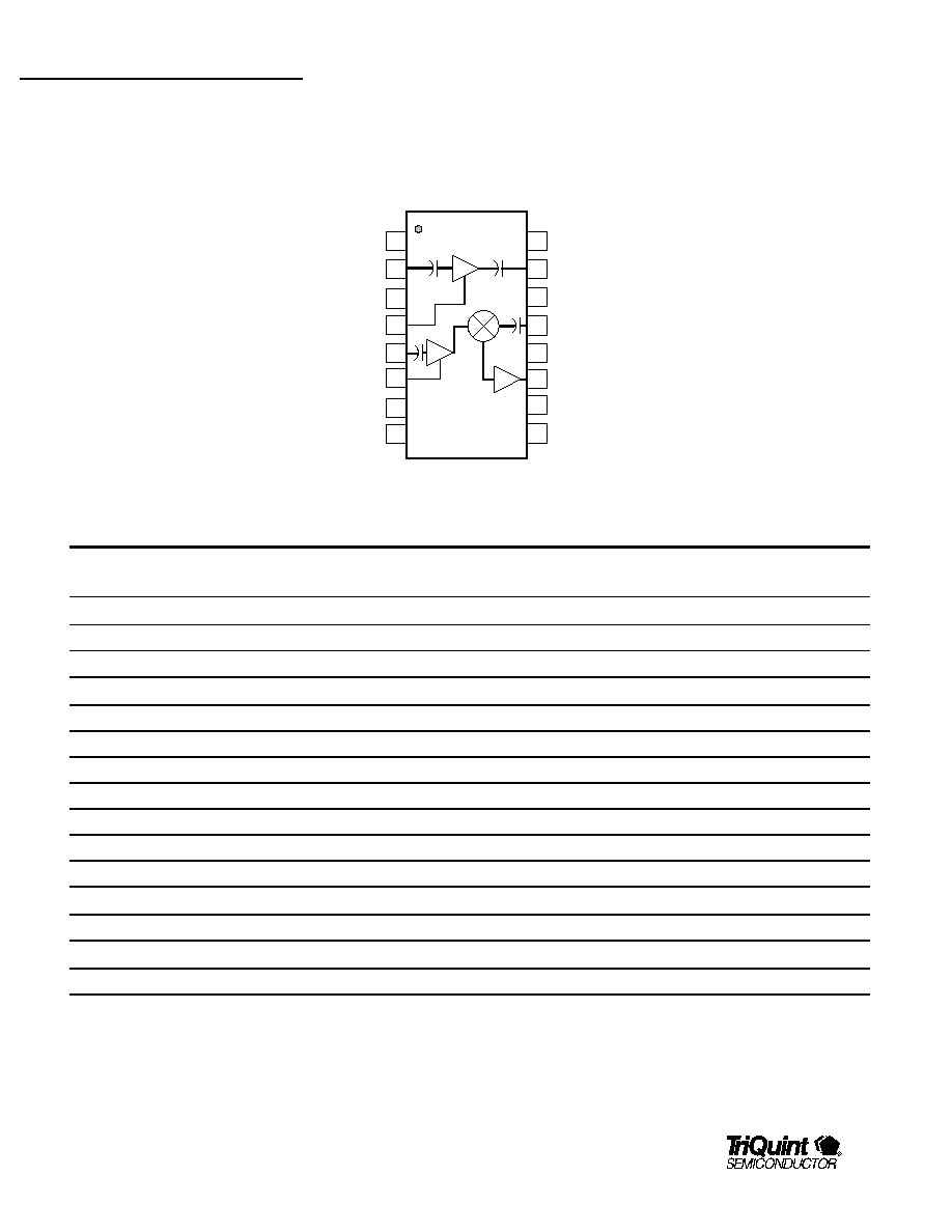
TQ5622 Product Description
The TQ5622 3V RFIC Downconverter is designed specifically
for PCS band TDMA applications. The TQ5622 contains LNA,
Mixer and LO buffer circuits matched to the 1900 MHz US PCS
frequency band. Any IF frequency may be selected between 85
and 150 MHz. Most RF ports are internally matched to 50
simplifying the design and minimizing the number of external
components. The TQ5622 also includes a power�down mode
switch which allows current saving during standby and the non-
operating portion of the TDMA pulse.
Operation
Please refer to the test circuit above.
Low Noise Amplifier (LNA)
The LNA section of the TQ5622 are cascaded common source
FET's, see Figure 1. It is designed to operate on DC supply
voltages from 2.7V to 5V. The source terminal must be
grounded as close as possible to Pin 1 to avoid significant gain
reduction due to degeneration. The LNA requires an input
matching circuit to obtain best noise figure, gain and return loss.
The LNA output is close to 50
for direct connection to a 50
image reject filter.
LNA
out
LNA
in
Vdd
BIAS
BIAS
LOAD
Figure 1. Simplified Schematic of LNA Section
LNA Input Match
The designer can make some Noise Figure and Gain trade off
by varying the off chip LNA input matching circuit values and
topology. This allows the TQ5622 to be optimized for specific
system requirements.
The LNA gain, noise figure and input return loss are a function
of the source impedance (Z
s
), or reflection coefficient (
s
),
presented to the input pin. Highest gain and lowest return loss
occur when
s
is equal to the complex conjugate of the LNA
input impedance. A different source reflection coefficient,
opt
,
which is experimentally determined, will provide the lowest noise
figure, F
min
.
The noise resistance, R
n
, provides an indication of the sensitivity
of the noise performance to changes in
s
as seen by the LNA
input.
(
)
F
F
R
Z
s
LNA
MIN
N
opt
S
opt
=
+
-
+
-
4
1
1
0
2
2
2
Components such as filters and mixers placed after the LNA
degrade the overall system noise figure according to the
following equation:
F
F
F
G
SYSTEM
LNA
LNA
=
+
-
2
1
F
LNA
and G
LNA
represent the linear noise factor and gain of the
LNA and F
2
is the noise factor of the next stage. The system
noise figure is a compromise between the highest gain and
minimum noise figure of the LNA. See Table 1 for noise
parameters.
Table 1. TQ5622 Noise Parameters
Freq. MHz
|Gopt|
/ Gopt
Fmin
Rn
1930
0.70
97
1.2
17
1960
0.70
94
1.2
18
1990
0.69
91
1.2
19
LNA Output Match
The output impedance of the LNA was designed for 50
. The
internal 50
match eliminates the need for external
components at this port. It also improves IP3 performance and
power gain.
The output of the LNA is intended to be connected directly to an
image reject filter. Depending on the filter, additional
components may be needed to better match to the LNA output.
Some image reject filters may require a series inductor to
smooth the frequency response and improve overall
performance.
TQ5622
Data Sheet
6
For additional information and latest specifications, see our website: www.triquint.com
Mixer
The mixer of the TQ5622 uses a common source depletion
mode MESFET. The mixer is designed to operate on supply
voltages from 2.7V to 5V. A 50
matched on-chip buffer
amplifier allows direct connection of the LO input to
commercially available VCO's with output drive levels as low as
-7dBm. The LO buffer provides good input match and supplies
the voltage gain needed to drive the mixer FET. The mixer also
has an "open-drain" IF output which provides flexibility in
matching to various IF frequencies and filter impedances, see
Figure 2.
LO Bias
and
Tuning
Mixer RF
Input
LO Input
Open Drain
IF Output
Figure 2, Mixer Section
LO Input Port
The LO input port is matched to 50
. This allows the TQ5622
to operate at low LO drivel levels. However, the position of C3
shown in the applications circuit may effect the gain of the LO
buffer amplifier, it should be placed as close as practicable to
Pin 6.
The buffer amplifier provides the voltage gain needed to drive
the gate of the mixer FET while using very little current
(approximately 1.5mA).
Because of the 50
input match of the buffer amplifier and the
internal DC blocking capacitor, the system VCO output can be
directly connected to the TQ5622 LO input via a 50
transmission line with no additional components.
Mixer Input
TriQuint has found that LO leakage through the Mixer RF input
pin, can in some cases, reflect off the SAW image reject filter
and return back to the mixer out of phase. This may cause
some degradation in conversion gain and system noise figure.
Sensitivity to the phenomena depends on the particular filter
model and the line length between the mixer input pin and the
filter. In some cases a small inductance can be added between
the filter and the mixer input to compensate. With some line
lengths and filter combinations, no inductor is necessary.
Mixer IF Port
The Mixer IF output is an "open-drain" configuration, allowing
flexibility in matching to various filter types and various IF
frequencies.
For evaluation of the LNA and mixer, it is usually necessary to
impedance match the IF port to the 50
test system. When
verifying or adjusting the matching circuit on the prototype circuit
board, the LO drive should be injected at pin 5 at the nominal
power level of -4 dBm, since the LO level does have an impact
on the IF port impedance.
There are several networks that can be used to properly match
the IF port to the SAW or ceramic IF filter. The mixer supply
voltage is applied through the IF port, so the matching circuit
topology must contain either an RF choke or shunt inductor. An
extra DC blocking capacitor is not necessary if the output will be
attached directly to a SAW or ceramic bandpass filter.
Figure 3 illustrates a shunt L, series C, shunt C IF matching
network. It is one of the simplest matching networks and
requires the fewest components. DC current can be easily
injected through the shunt inductor and the series C provides a
DC block, if needed. The shunt C, is used to reduce the LO
leakage.
IF out
V IF
100nH
10 pF
1000pF
Pin 11
Pin 10
15pF
Figure 3, IF Output Match, 135 MHz
Power down, "sleep" mode
The power down circuit is used to reduce average power
consumption of the receiver in TDMA applications by toggling
the receiver on and off within the TDMA receive time slot when
no signal is present. The power down circuitry operates through

TQ5622
Data Sheet
For additional information and latest specifications, see our website: www.triquint.com
7
the incorporation of enhancement-mode FET switches in all DC
paths. Level shifting circuitry is incorporated to provide an
interface compatible with CMOS logic levels. The entire
TQ5622 chip nominally draws 100uA when the power-down pin
is at 0V. When the power-down pin is at 2.8V (Vdd), the chip
draws nominal specified current. The power-down pin itself, Pin
16, draws approximately 40uA when 2.8V is applied. Less than
1uA is sourced from the power-down pin when 0V is applied.
TQ5622
Data Sheet
8
For additional information and latest specifications, see our website: www.triquint.com
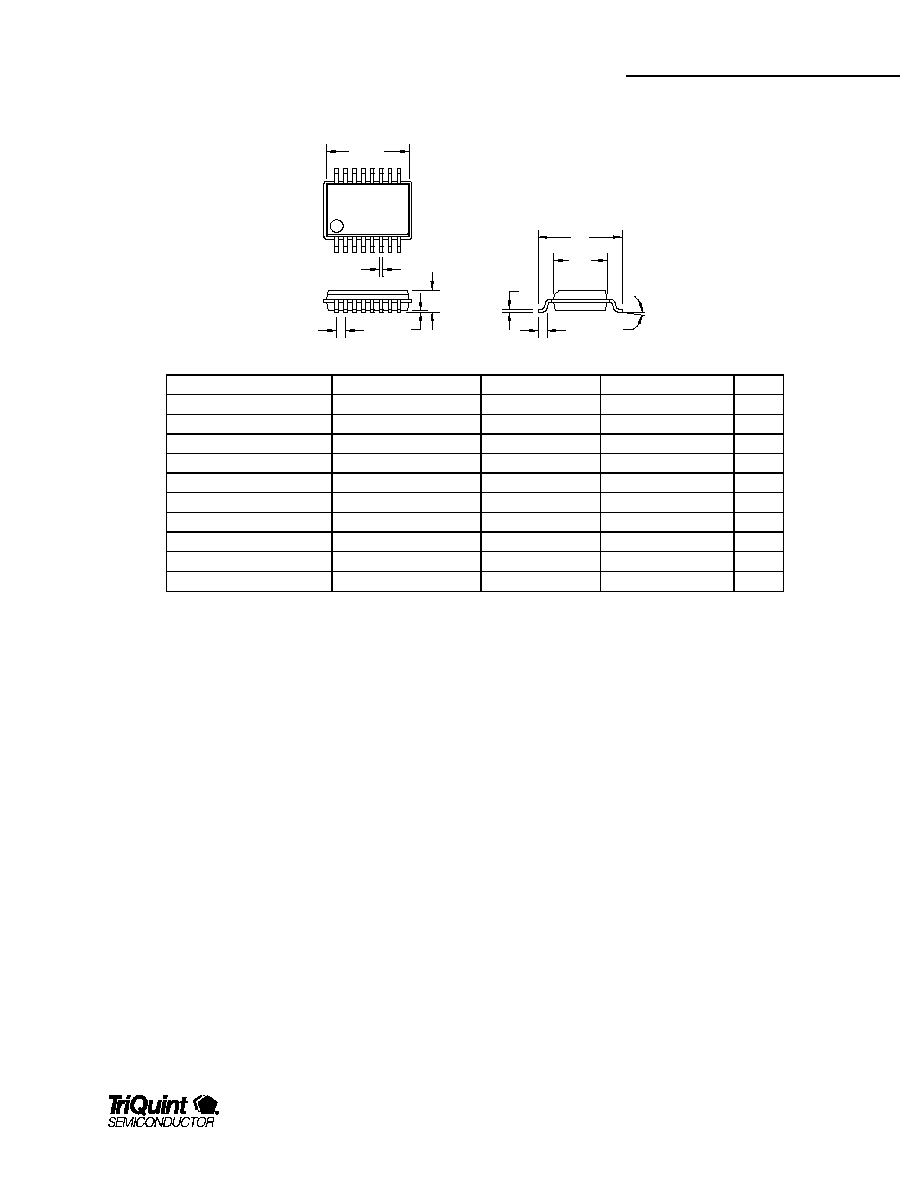
Package Pinout
LO IN
1
2
3
4
6
7
9
10
11
12
13
14
15
16
GND
GND
GND
Vdd MXR
5
VDD LNA
RF IN
Sleep
Control
IF OUT/Vdd
8
GND
GND
GND
GND
GND
LNA Out
MXR RF IN
Pin Descriptions
Pin Name
Pin #
Description and Usage
GND, LNA
1
LNA first stage ground connection. Direct connection to ground required.
LNA IN
2
LNA RF input. DC blocked. Requires external matching elements for noise match and match to 50
GND
3
Ground
V
DD
LNA
4
LNA DC supply voltage. Local external bypass capacitor required.
MXR LO IN
5
Mixer LO input. DC blocked, matched to 50
VDD_MXR
6
Mixer LO buffer supply voltage. Local external bypass capacitor required.
GND
7
Ground
GND
8
Ground
GND
9
Ground
GND
10
Ground
IF OUT
11
IF output. Open drain output, connection to Vdd required. External matching is required.
GND
12
Ground
MXR_RF
13
Mixer RF input, DC blocked. Matched to 50
.
GND
14
Ground
LNA OUT
15
LNA RF Output. DC blocked. Matched to 50
.
SLEEP
16
Power-Down mode control.
For ground pins 1,3,7,8,9,10,12, and 14, TriQuint recommends use of several via holes to the backside ground immediately adjacent to the
pin.
Package Type: Power QSOP-16 Plastic Package
TQ5622
Data Sheet
Additional Information
For latest specifications, additional product information, worldwide sales and distribution locations, and information about TriQuint:
Web: www.triquint.com
Tel: (503) 615-9000
Email: info_wireless@tqs.com
Fax: (503) 615-8900
For technical questions and additional information on specific applications:
Email: info_wireless@tqs.com
The information provided herein is believed to be reliable; TriQuint assumes no liability for inaccuracies or omissions. TriQuint assumes no responsibility for the use of
this information, and all such information shall be entirely at the user's own risk. Prices and specifications are subject to change without notice. No patent rights or
licenses to any of the circuits described herein are implied or granted to any third party.
TriQuint does not authorize or warrant any TriQuint product for use in life-support devices and/or systems.
Copyright � 1999 TriQuint Semiconductor, Inc. All rights reserved.
Revision A, September 20, 1999
For additional information and latest specifications, see our website: www.triquint.com
9
D
NOTE A
e
b
E
E1
NOTE B
A
L
c
A1
DESIGNATION
DESCRIPTION
ENGLISH
METRIC
NOTE
A
OVERALL HEIGHT
0.064
+/-.005 in
1.63
+/-.13 mm
C
A1
STANDOFF
0.007
+/-.003 in
0.18
+/-.08 mm
C
b
LEAD WIDTH
0.010
+/-.002 in
0.25
+/-.05 mm
C
c
LEAD THICKNESS
0.085
+/-.015 in
2.16
+/-.38 mm
C
D
PACKAGE LENGTH
0.193
+/-.004 in
4.90
+/-.10 mm
A, C
e
LEAD PITCH
0.025
BSC
0.635
BSC
E
LEAD TIP SPAN
0.236
+/-.008 in
5.99
+/-.20 mm
C
E1
PACKAGE WIDTH
0.154
+/-.003 in
3.91
+/-.08 mm
B, C
L
FOOT LENGTH
0.033
+/-.017 in
0.84
+/-.43 mm
C
FOOT ANGLE
4
+/-4 DEG
4
+/-4 DEG
NOTES:
A.
The D dimension does not include mold flashing and mismatch. Mold flashing and mismatch shall not exceed .006 in (.15 mm) per
side.
B.
The E1 dimension does not include mold flashing and mismatch. Mold flashing and mismatch shall not exceed .010 in (.25 mm)
per side.
C.
Primary units are English inches. The metric equivalents are subject to rounding error.