WIRELESS COMMUNICATIONS DIVISION
For additional information and latest specifications, see our website: www.triquint.com
1
TQ5132
DATA SHEET
3V Cellular Band
CDMA/AMPS RFA/Mixer
IC
Features
Small size: SOT23-8
Single 3V operation
Low-current operation
Gain Select
Mode Select
High IP3 performance
Few external components
Applications
IS-95 CDMA Mobile Phones
AMPS Mobile Phones
Dual Mode CDMA Cellular application
Product Description
The TQ5132 is a 3V, RFA/Mixer IC designed specifically for Cellular band
CDMA/AMPS applications. It's RF performance meets the requirements of products
designed to the IS-95 and AMPS standards. The TQ5132 is designed to be used
with the TQ3131 or TQ3132 (CDMA/AMPS LNA) which provides a complete CDMA
receiver for 800MHz dual-mode phones.
The RFA/Mixer incorporates on-chip switches which determine CDMA, AMPS and
bypass mode select. When used with the TQ3131 or TQ3132 (CDMA/AMPS LNA),
four gain steps are available. The RF input port is internally matched to 50
,
greatly simplifying the design and keeping the number of external components to a
minimum. The TQ5132 achieves good RF performance with low current
consumption, supporting long standby times in portable applications. Coupled with
the very small SOT23-8 package, the part is ideally suited for Cellular band mobile
phones.
Electrical Specifications
1
Parameter
Min
Typ
Max
Units
Frequency
881
MHz
Gain
15.0
dB
Noise Figure
4.5
dB
Input 3
rd
Order Intercept
2.5
dBm
DC supply Current
15.0
mA
Note 1: Test Conditions: Vdd=2.8V, RF=881MHz, LO=966MHz, IF=85MHz, Ta=25C, CDMA High Gain
state.
RF
IN
VDD
LO
GND
GIC
IF
Out
AMPS
IF Out
IN
Mode Select/
LO Input
IF
Out
IFA Gain
Select
CDMA
IF Out
Control 2
Control 1
Control 3
RFA Gain
Select

TQ5132
Data Sheet
2
For additional information and latest specifications, see our website: www.triquint.com
Electrical Characteristics
Parameter
Conditions
Min.
Typ/Nom
Max.
Units
RF Frequency
Cellular band
869
881
894
MHz
IF Frequency Range
High side LO
85
130
MHz
CDMA Mode-High Gain
Gain
12.6
16.0
18.2
dB
Noise Figure
4.5
7.2
dB
Input IP3
-2.2
2.5
dBm
Supply Current (T
A
= 25
�
C)
18.0
21.0
mA
CDMA Mode-High Gain Low Linearity
Gain
18.5
dB
Noise Figure
4.0
dB
Input IP3
-0.3
dBm
Supply Current (T
A
= 25
�
C)
18.0
mA
CDMA Mode-Mid Gain
Gain
5.0
dB
Noise Figure
11.0
dB
Input IP3
14.0
dBm
Supply Current (T
A
= 25
�
C)
13.5
mA
CDMA Mode-Low Gain
Gain
5.2
8.0
10.2
dB
Noise Figure
10.0
12.8
dB
Input IP3
7.4
11.0
dBm
Supply Current (T
A
= 25
�
C)
14.0
17.5
mA
AMPS Mode
Gain
7.7
12.0
12.6
dB
Noise Figure
5.0
7.7
dB
Input IP3
-4.9
-1.0
dBm
Supply Current (T
A
= 25
�
C)
9.0
10.3
mA
Supply Voltage
2.8
3.15
V
Note 1: Test Conditions: Vdd=2.8 to 3.15V, RF=869-894MHz, LO=High side �6 to �2dBm, IF=85MHz, T
A
= -30 to 85
�
C, unless otherwise specified.
Absolute Maximum Ratings
Parameter
Value
Units
DC Power Supply
5.0
V
Power Dissipation
500
mW
Operating Temperature
-30 to 85
C
Storage Temperature
-60 to 150
C
Signal level on inputs/outputs
+20
dBm
Voltage to any non supply pin
+0.3
V
TQ5132
Data Sheet
For additional information and latest specifications, see our website: www.triquint.com
3
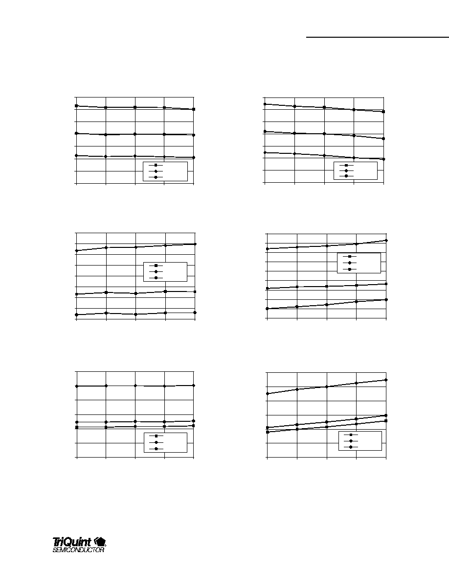
Typical Performance,
Note: HG Mode=CDMA High Gain, LG Mode=CDMA Low Gain
Test Conditions, unless otherwise specified: Vdd=2.8V, Ta=25C, RF=881MHz, LO=966MHz, LO input=-4dBm, IF=85MHz
Gain vs. Frequency
4
6
8
10
12
14
16
18
869
875
882
888
894
Frequency (MHz)
Gai
n
(
d
B)
HG Mode
LG Mode
AMPS
Gain vs. Temperature
4
6
8
10
12
14
16
18
-30
0
25
55
85
Temperature (Celsius)
Ga
in (dB)
HG Mode
LG Mode
AMPS
Input IP3 vs. Frequency
-2
0
2
4
6
8
10
12
14
869
875
882
888
894
Frequency (MHz)
I
nput
I
P
3 (
d
Bm)
HG Mode
LG Mode
AMPS
Noise Figure vs. Frequency
0
2
4
6
8
10
12
869
875
882
888
894
Frequency (MHz)
Noi
se Fi
gur
e (
d
B)
HG Mode
LG Mode
AMPS
Input IP3 vs. Temperature
-4
-2
0
2
4
6
8
10
12
14
-30
0
25
55
85
Temperature (Celsius)
I
nput
I
P
3 (
d
Bm)
HG Mode
LG Mode
AMPS
Noise Figure vs. Temperature
0
2
4
6
8
10
12
-30
0
25
55
85
Temperature (Celsius)
Noi
se Fi
gur
e (
d
B)
HG Mode
LG Mode
AMPS

TQ5132
Data Sheet
4
For additional information and latest specifications, see our website: www.triquint.com
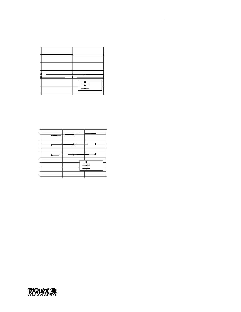
Idd vs. Temperature
0
2
4
6
8
10
12
14
16
18
20
-30
0
25
55
85
Temperature (Celsius)
I
dd (
m
A)
HG Mode
LG Mode
AMPS
Gain vs. LO Power
0
2
4
6
8
10
12
14
16
18
-6
-4
-2
LO Power (dBm)
G
a
in
(d
B
)
HG Mode
LG Mode
AMPS
Input IP3 vs. LO Power
-4
-2
0
2
4
6
8
10
12
14
-6
-4
-2
LO Power (dBm)
I
nput
I
P
3 (
d
Bm)
HG Mode
LG Mode
AMPS
Noise Figure vs. LO Power
0
2
4
6
8
10
12
-6
-4
-2
LO Power (dBm)
Noi
se Fi
gur
e (
d
B)
HG Mode
LG Mode
AMPS
Gain vs. Vdd
3
6
9
12
15
18
2.8
3
3.15
Vdd (volts)
Gai
n
(
d
B)
HG Mode
LG Mode
AMPS
Input IP3 vs. Vdd
-2
0
2
4
6
8
10
12
14
2.8
3
3.15
Vdd (volts)
I
nput
I
P
3 (
d
Bm)
HG Mode
LG Mode
AMPS
TQ5132
Data Sheet
For additional information and latest specifications, see our website: www.triquint.com
5
Noise Figure vs. Vdd
0
2
4
6
8
10
12
2.8
3
3.15
Vdd (volts)
Noi
se Fi
gur
e (
d
B)
HG Mode
LG Mode
AMPS
Idd vs. Vdd
0
2
4
6
8
10
12
14
16
18
20
2.8
3
3.15
Vdd (volts)
I
dd (
m
A)
HG Mode
LG Mode
AMPS

TQ5132
Data Sheet
6
For additional information and latest specifications, see our website: www.triquint.com
Application/Test Circuit
Bill of Material for TQ5132 RF AMP/Mixer
Component
Reference Designator
Part Number
Value
Size
Manufacturer
Receiver IC
U1
TQ5132
SOT23-8
TriQuint Semiconductor
Capacitor
C4
.022
�
F
0402
Capacitor
C10
18pF
0402
Capacitor
C5,C8
1200pF
0402
Capacitor
C6
27pF
0402
Capacitor
C7
30pF
0402
Capacitor
C9
15pF
0402
Capacitor
C12
100pF
0402
Capacitor
C22
2.7pF
0402
Resistor
R1, R4
5.1K
0402
Resistor
R2
6.8
0402
Resistor
R3
180
0402
Inductor
L2
180nH
0805
Inductor
L3
270nH
0805
Inductor
L4
18nH
0402
RF
IN
VDD
LO
Mode Select
GND
RF input
GIC
IF
Out
IF Out
VDD
AMP's
IF Out
IN
Gain
Select
VDD
RF AMP
Mixer
C4
C6
C7
C5
C9
R1
L2
CDMA
IF
Out
VDD
C8
L3
C10
C12
R4
IF AMP
Gain
Select
C22
L4
Control 2
R2
R3
Control 3
Control 1
LO
INPUT
TQ5132
Data Sheet
For additional information and latest specifications, see our website: www.triquint.com
7
TQ5132 Product Description
The TQ5132 is a miniature low noise mixer (downconverter) in a
small SOT-23-8 package (2.9X2.8X1.14 mm) with operation at
2.8v. The TQ5132 specs are designed to be compatible with IS-
98 Interim Standard for Dual-Mode CDMA cellular systems. The
low noise mixer features an AMPS control pin for Gain, Intercept
and Current (GIC pin) and it has excellent intermodulation
characteristics with high intercept point in all modes. For
optimum performance the TQ5132 RF frequency of operation
should be from 869 to 894 MHz. The IF range is from 85 to 130
MHz and its injection mode for the local oscillator is high side.
Operation
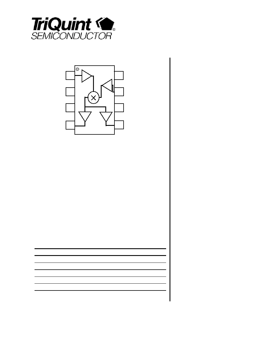
The TQ5132 is a single-ended mixer with switching capabilities
for the various signal levels found in CDMA applications. The
TQ5132 combines a RF amplifier, a LO driver amplifier, and
separate digitally controlled IF amplifiers for CDMA and AMPS
outputs.
2
1
4
5
6
8
3
7
RF / C2
Mx Vdd
GND
GIC
CDMA
IF
Output
IFA GS / C3
LO / C1
AMPS
IF
Output
TQ5132
Figure 1. TQ5132 Block Diagram
Circuit Description
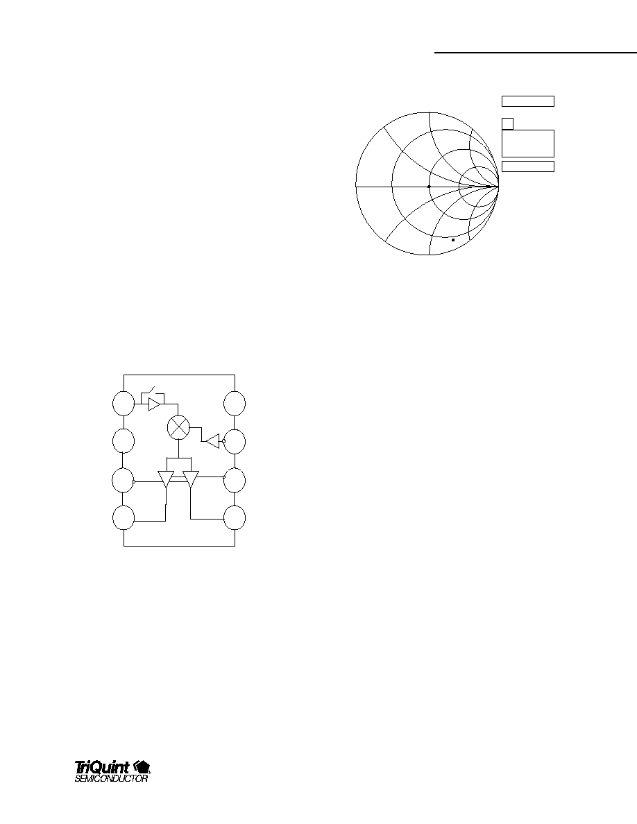
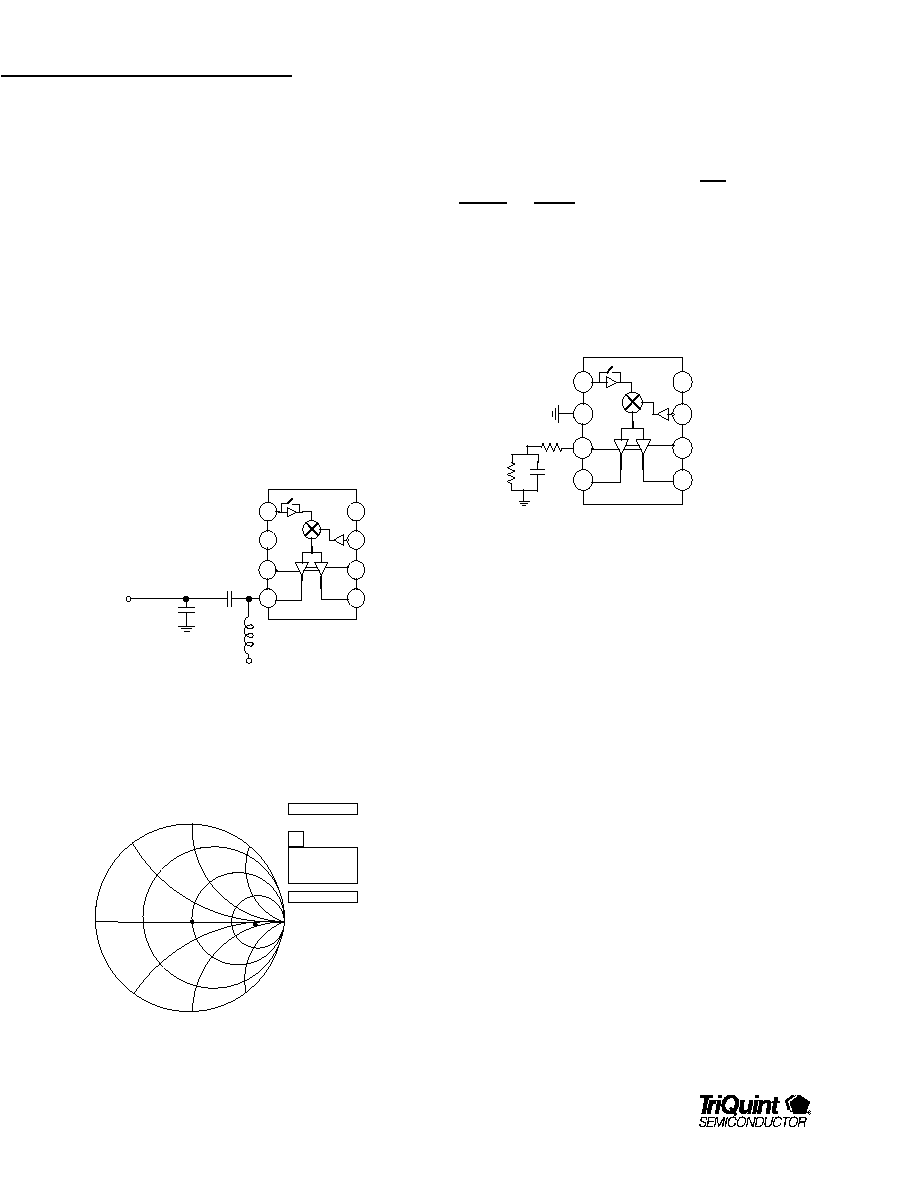
RF Amplifier
The TQ5132 has an integrated pre-amplifier stage in a cascode
configuration. The output is internally matched to 50 ohms at
881MHz. Pin 1 requires an external match that is set to deliver a
2:1 VSWR in both the low and high gain modes (i.e. RFA is on
or off). Figure 2 shows an approximated impedance at pin 1
(RFA input) to implement any desired match. Remember to
apply the LO signal when tuning the RF match.
2.0
1.0
0.5
-0.5
-1.0
-2.0
1.0
2.0
0.5
A
0.76 @ -65.5
z = 0.44 - j 1.46
y = 0.19 + j 0.63
A
Input
Impedance
Freq=881MHz
TQ5132
Figure 2. TQ5132 RF Amplifier Input Impedance
LO Buffer Amplifier
The LO buffer amplifier is a grounded gate FET with a
broadband match to 50
. It has on-chip DC block and on-chip
LO tuning circuit to shape the frequency response and drive it to
a level suitable for the gate of the mixer FET. Thus the optimum
LO frequency range is fixed and centered around 990mhz. The
LO is limited to high-side injection mode and it operates from
950MHz to 1030MHz. The input to the LO buffer is through pin 7
which also feeds the control line (C1) that selects the mixer
mode of operation, either CDMA or AMPS. Due to this logic
control, the only external component required at the LO port is a
series capacitor to prevent DC from traveling to other parts of
the system. The LO drive level of operation should be between -
7 and 0 dBm. Best performance is obtained between �6 and �
2 dBm.
LO/filter/Mixer interaction
The physical position of the image reject filter is likely to have an
effect on the performance of the mixer especially in the Low
Gain mode where the RF amplifier is switched out. This is
primarily due to self-mixing of the LO energy bouncing from the
filter back into the mixer either out-of-phase or in-phase creating
an offset in magnitude. To minimize this effect, TriQuint
recommends placing the image-reject filter as close to the IC as
possible. In TriQuint's demo board its position is 42 mils from
the pad of the matching inductor and 126 mils from the IC pad.
This location for the image-reject filter works well.
TQ5132
Data Sheet
8
For additional information and latest specifications, see our website: www.triquint.com
CDMA IF Amplifier
The CDMA IF amplifier is an open drain stage with a gain step
to adjust the output power levels according to the system
requirement. No quiescent current adjustments are possible in
this mode since the self-bias circuit is on-chip. While the IF
output can be tuned for frequencies as high as 500 MHz, the
downconverter performance is limited by the internal tuned
circuit of the LO buffer amplifier. The highest IF that can be used
without significant deviation from typical performance is 130
MHz. This output is a high impedance open drain FET z = 5.47
� j 0.71
(normalized). The match requires a RF choke to Vdd
for proper biasing (see figure 3). Typical CDMA IF output
impedance is shown in figure 4. The gain of the CDMA IF
amplifier can be adjusted according to the degeneration resistor
value R2 (see figure 5).
Note: These values were optimized for TriQuint's 5131 Demo
board. The discrepancy between these values and those of the
customer's application may differ due to board and component
parasitics.
Vdd
L2=180nH
2
1
4
5
6
8
3
7
CDMA
IF
Output
TQ5132
C7=30pF
C6=27pF
Figure 3. TQ5132 CDMA IF Output Match (IF = 85MHz)
2.0
1.0
0.5
-0.5
-1.0
-2.0
1.0
2.0
0.5
B
0.70 @ -2.8
z = 5.47- j 0.71
y = 0.18 + j 0.02
B
CDIF output
Impedance
TQ5132
Freq=85MHz
Figure 4. TQ5132 CDMA IF Output Impedance at Pin 4
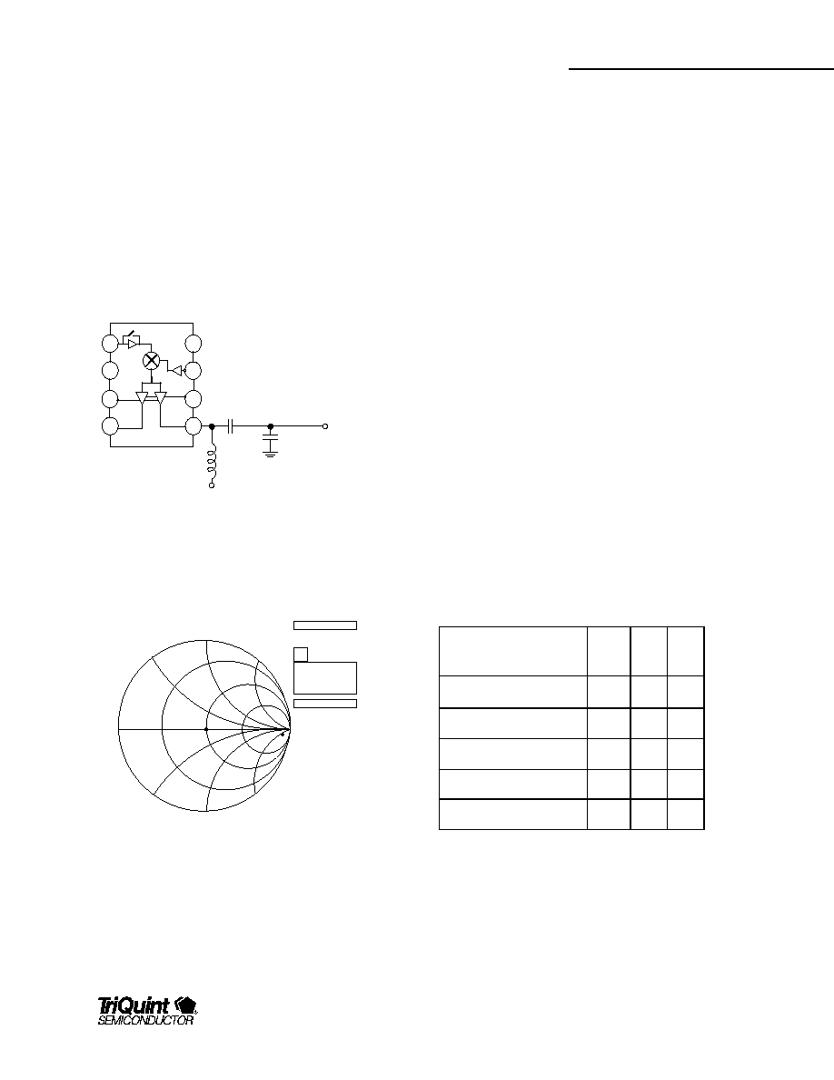
AMPS IF Amplifier
The source of the AMPS IF amplifier is connected directly to pin
3. This allows the system designer to adjust Gain, output
Intercept and Current (GIC) by adding an external self-bias
circuit at this pin (see figure 5). A large bypass capacitor value
in the self-bias circuit minimizes the effects of low frequency
components present at this pin. TriQuint recommends 0.022uF
or greater. The AMPS IF amplifier gain is only mildly affected by
the value of R2.
Note: These values were optimized for TriQuint's 5131 Demo
board. The discrepancy between these values and those of the
customer's application may differ due to board and component
parasitics.
2
1
4
5
6
8
3
7
TQ5132
C4 = 0.022uF
R2
R3
C4
R2 = 6.8
R3 = 180
Figure 5. TQ5132 AMPS GIC pin
Once the operating point is chosen, the designer still has
flexibility to adjust gain and intercept by varying the ratio of the
DC bias resistors, R2/R3. Maximum gain is obtained when the
total DC resistance (R2 + R3) at pin 3 is bypassed.
The normalized impedance of the AMPS IF output is z = 15.4 � j
2.87
. This particular measurement was taken on the 5132
demo board by lifting pin 5 of the PCB pad and soldering the
center conductor of a semirigid probe next to it. The outer
conductor was grounded close to the pin and its electrical length
dialed as a port extension in order to move the calibration
reference plane right at the tip of the probe. Keep in mind that
the total DC bias resistance in the GIC pin must be selected
before taking this measurement. When designing the PCB, it is
recommended to place the self-bias circuit of the amplifier as
close to the pin as possible to minimize possible loading effects
that might cause oscillation. Similarly, the shunt capacitor C10
TQ5132
Data Sheet
For additional information and latest specifications, see our website: www.triquint.com
9
of the IF match should be grounded close to the IC (see figure
6).
After designing the IF match in simulation using the given S-
parameters, some adjustment might be needed when
implementing the match on the bench. At this point remember
that the LO driver amplifier must be turned on since the IFA is
directly coupled to the mixer FET. Figure 6 shows the circuit
topology and component values designed for TriQuint's demo
board. Figure 7 shows a typical AMPS IF output impedance.
Note: These values were optimized for TriQuint's 5131 Demo
board. The discrepancy between these values and those of the
customer's application may differ due to board and component
parasitics.
Vdd
L3=270nH
2
1
4
5
6
8
3
7
TQ5132
AMPS
IF
Output
C10=18pF
C9=15pF
Figure 6. TQ5132 AMPS IF Output Match (IF = 85 MHz)
2.0
1.0
0.5
-0.5
-1.0
-2.0
1.0
2.0
0.5
C
0.9 @ - 2.9
z = 15.4 - j 7.23
y = 0.05 + j 0.02
C
AMIF output
Impedance
Freq=85MHz
TQ5132
Figure 7. TQ5132 AMPS IF Output Impedance at Pin 5
Vdd Decoupling
External spurious signals at high and low frequencies can
appear on the Vdd lines. Proper decoupling of these lines is
required to eliminate unwanted noise. The recommended
decoupling network has a PI configuration. On the main Vdd
node, a large capacitor of 0.022 uF is used, followed by a 3.3 or
10 ohm resistor in series with the supply line. Last, a bypass
capacitor that presents a low impedance to ground at the RF
frequency is normally placed very close to the pin. However, in
the TQ5132 this bypass capacitor on the IC node is on-chip and
the external one near the IC is not needed.
Board Layout Recommendations
All ground pins should be kept close to the IC and have its own
via to the ground plane to minimize inductance.
Most PC boards for portable applications have thin dielectric
layers and very narrow line width which increase the board
parasitic capacitance and inductance. To minimize these effects
when implementing a matching network, it is recommended to
relieve the ground underneath pads carrying RF signals
whenever possible.
Control Line Description
The control lines can be toggled between high and low levels
using CMOS logic circuitry. Control line C1 is used to switch
between CDMA and AMPS IF output. The other two control
lines C2 and C3 set the various CDMA output levels required by
the system.
Table 1. Downconverter Control Lines C1, C2, C3
Receiver State
C1
C2
C3
AMPS Mode
0
0
1
CDMA High Gain
1
0
0
CDMA HG, low lin
1
0
1
CDMA Mid Gain
1
1
0
CDMA Low Gain
1
1
1
C1 = Mixer Mode, C2 = RFA gain select and LNA gain select,
C3 = IFA gain select and LNA mode select.

TQ5132
Data Sheet
10
For additional information and latest specifications, see our website: www.triquint.com
Receiver State
RFA
IFA
AMPS Mode
HG, AMPS Idd
HG, AMPS Output
CDMA High Gain
HG, CDMA Idd
LG, CDMA Output
CDMA HG, low lin
HG, CDMA Idd
HG, CDMA Output
CDMA Mid Gain
Bypass
LG, CDMA Output
CDMA Low Gain
Bypass
HG, CDMA Output
Table 2. Electrical States of RFA and IFA
In the AMPS mode the TQ5132 switches the IF output to the
AMPS pin and turns on the RF amplifier but at lower current
than CDMA mode. Thus the system draws much less current
in AMPS mode.
In the High Gain modes, a cascode amplifier is switched in
before the mixer. Control for this function is made via a DC
signal on the RF input pin 1. The IF amplifier gain can be
stepped as well via a control line at pin 6.
The CDMA Mid Gain Mode provides an intermediate gain step.
The mixer has the RF amplifier turned off and the IF stage at
minimum gain.
In the low gain modes, the RF amplifier is disabled and the input
signal is routed directly to the mixer.
TQ5132
Data Sheet
For additional information and latest specifications, see our website: www.triquint.com 9
Package Pinout
Pin Descriptions
Pin Name
Pin #
Description and Usage
RF IN
1
RF Input, RF amplifier gain select, Logic Control 2
GND
2
Ground, paddle
GIC
3
Off chip tuning for gain/IP3/current
IF OUT
4
CDMA IF Output
IF OUT
5
AMPS IF Output
IFA Gain
6
IF amplifier gain select, Logic Control 3
LO IN
7
LO Input, mode select (CDMA/AMPS), Logic Control 1
Vdd
8
LNA Vdd, typical 2.8V
RF
IN
VDD
LO
GND
GIC
IF
Out
AMP's
IF Out
IN
Mode Select/
LO Input
IF
Out
IFA Gain
Select
CDMA
IF Out
Control 2
Control 1
Control 3
TQ5132
Data Sheet
Additional Information
For latest specifications, additional product information, worldwide sales and distribution locations, and information about TriQuint:
Web: www.triquint.com
Tel: (503) 615-9000
Email: info_wireless@tqs.com
Fax: (503) 615-8900
For technical questions and additional information on specific applications:
Email: info_wireless@tqs.com
The information provided herein is believed to be reliable; TriQuint assumes no liability for inaccuracies or omissions. TriQuint assumes no responsibility for the use of
this information, and all such information shall be entirely at the user's own risk. Prices and specifications are subject to change without notice. No patent rights or
licenses to any of the circuits described herein are implied or granted to any third party.
TriQuint does not authorize or warrant any TriQuint product for use in life-support devices and/or systems.
Copyright � 2000 TriQuint Semiconductor, Inc. All rights reserved.
Revision A, April, 2000
12
For additional information and latest specifications, see our website: www.triquint.com
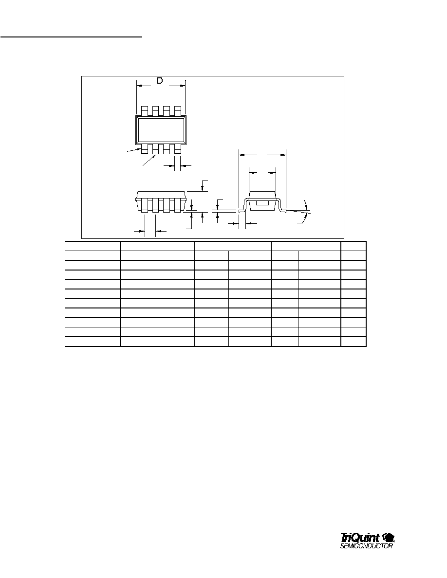
Package Type: SOT23-8 Plastic Package
DESIGNATION
DESCRIPTION
METRIC
ENGLISH
NOTE
A
OVERALL HEIGHT
1.20 +/-.25 mm
0.05 +/-.250 in
3
A1
STANDOFF
.100 +/-.05 mm
.004 +/-.002 in
3
b
LEAD WIDTH
.365 mm TYP
.014 in
3
c
LEAD THICKNESS
.127 mm TYP
.005 in
3
D
PACKAGE LENGTH
2.90 +/-.10 mm
.114 +/-.004 in
1,3
e
LEAD PITCH
.65 mm TYP
.026 in
3
E
LEAD TIP SPAN
2.80 +/-.20 mm
.110 +/-.008 in
3
E1
PACKAGE WIDTH
1.60 +/-.10 mm
.063 +/-.004 in
2,3
L
FOOT LENGTH
.45 +/-.10 mm
.018 +/-.004 in
3
Theta
FOOT ANGLE
1.5 +/-1.5 DEG
1.5 +/-1.5 DEG
Notes
1. The package length dimension includes allowance for mold mismatch and flashing.
2. The package width dimension includes allowance for mold mismatch and flashing.
3. Primary dimensions are in metric millimeters. The English equivalents are calculated and subject to rounding error.
E
L
A1
b
e
FUSED LEAD
c
A
Note 1
PIN 1
E1
Note 2
DIE