Äîêóìåíòàöèÿ è îïèñàíèÿ www.docs.chipfind.ru
TriQuint Semiconductor Texas : (972)994 8465 Fax (972)994 8504 Web: www.triquint.com
1
Advance Product Information
May 3, 2000
18 - 20 GHz 5-Bit Phase Shifter TGC1439A-EPU
Key Features and Performance
·
0.5um pHEMT Technology
·
18-20 GHz Frequency Range
·
3º Typical RMS Phase Shift Error
·
-5 dB Typical Insertion Loss
·
Control Voltage: -2.5 V to -5.0 V
·
Compact 1.27 mm
2
Die Area
Primary Applications
·
Phased Arrays
·
Satellite Communication Systems
The TriQuint TGC1439A-EPU is a 5-Bit Digital Phase
Shifter MMIC design using TriQuint's proven 0.5
µm
Power pHEMT process to support a variety of K-Band
phased array applications including satellite
communication systems.
The 5-bit design utilizes a compact topology that
achieves a 1.27 mm
2
die area, high performance and
good tolerance to control voltage variation
The TGC1439A provides a 5-Bit digital phase shift
function with a nominal -5 dB insertion loss and 3º
RMS phase shift error over a bandwidth of 18-20 GHz.
The TGC1439A requires a minimum of off-chip
components and operates with a -5.0 V to -2.5 V
control voltage range. Each device is RF tested on-
wafer to ensure performance compliance. The device
is available in chip form.
Note: Devices designated as EPU are typically early in their characterization process prior to finalizing all electrical and process
specifications. Specifications are subject to change without notice.
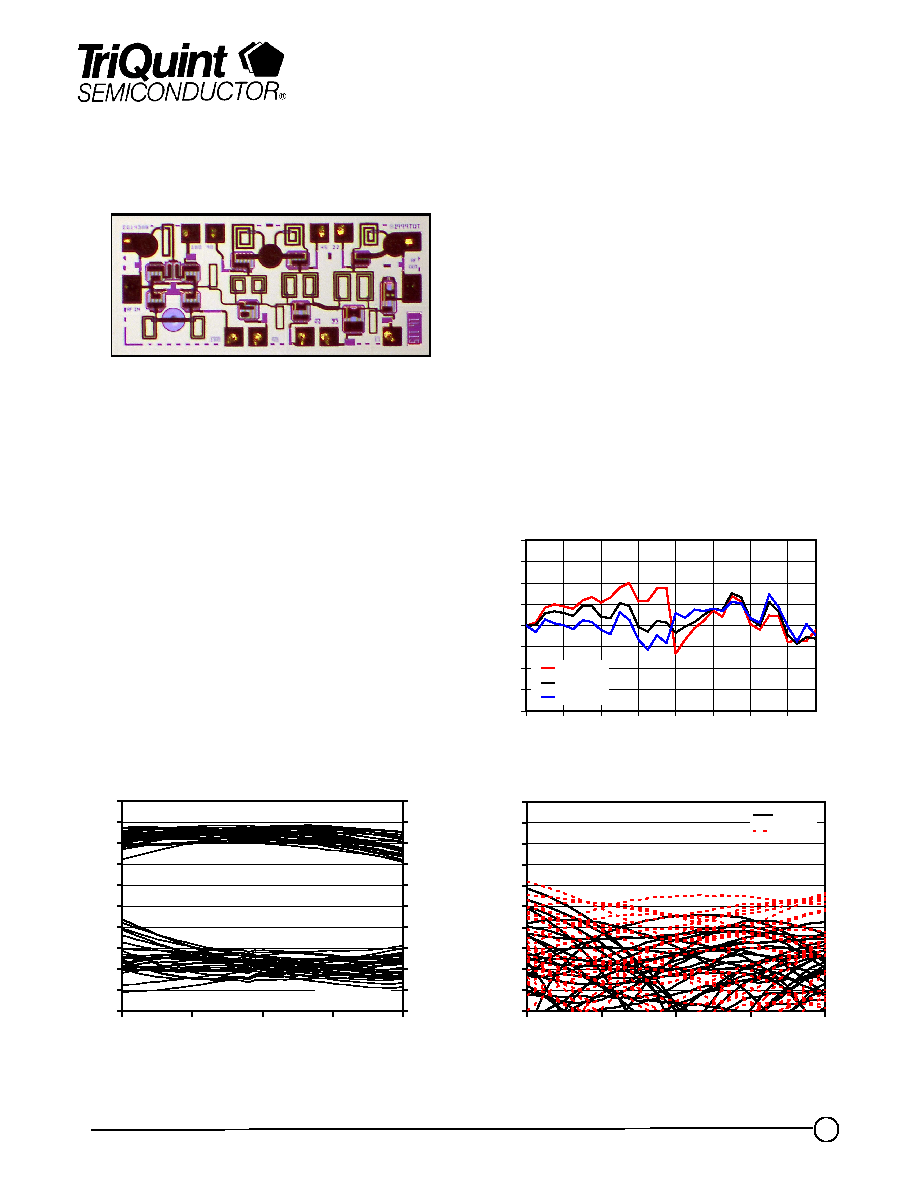
TGC1439A Typical RF Performance (Fixtured)
-20
-18
-16
-14
-12
-10
-8
-6
-4
-2
0
17
18
19
20
21
Frequency (GHz)
Return Loss (
d
B)
Input
Output
-13
-12
-11
-10
-9
-8
-7
-6
-5
-4
-3
17
18
19
20
21
Frequency (GHz)
In
se
rtion
Loss (
d
B)
-10
-5
0
5
10
15
20
25
30
35
40
Ph
ase
S
h
i
f
t
Error (
d
e
g
)
Insertion Loss
Phase Error
TGC1439A Typical RF Performance (Fixtured)
TGC1439A Typical RF Performance (Fixtured)
-12
-9
-6
-3
0
3
6
9
12
0
4
8
12
16
20
24
28
Phase State
Ph
ase
S
h
i
f
t
Error (
d
e
g
)
18 GHz
19 GHz
20 GHz
TriQuint Semiconductor Texas : (972)994 8465 Fax (972)994 8504 Web: www.triquint.com
2
Advance Product Information
May 3, 2000
RECOMMENDED MAXIMUM RATINGS
Symbol
Parameter
Value
Notes
V
-
Control Voltage
-8 V
I
+
Control Current
1 mA
3/
P
D
Power Dissipation
0.1 W
P
IN
Input Continuous Wave Power
20 dBm
T
CH
Operating Channel Temperature
150
°C
1/, 2/
T
M
Mounting Temperature (30 seconds)
320
°C
T
STG
Storage Temperature
-65
°C to 150 °C
1/
These ratings apply to each individual FET
2/
Junction operating temperature will directly affect the device mean time to failure
(MTTF). For maximum life it is recommended that junction temperatures be
maintained at the lowest possible levels.
3/
Total current for the entire MMIC
Electrical Characteristics
Note: Devices designated as EPU are typically early in their characterization process prior to finalizing all electrical and process
specifications. Specifications are subject to change without notice.
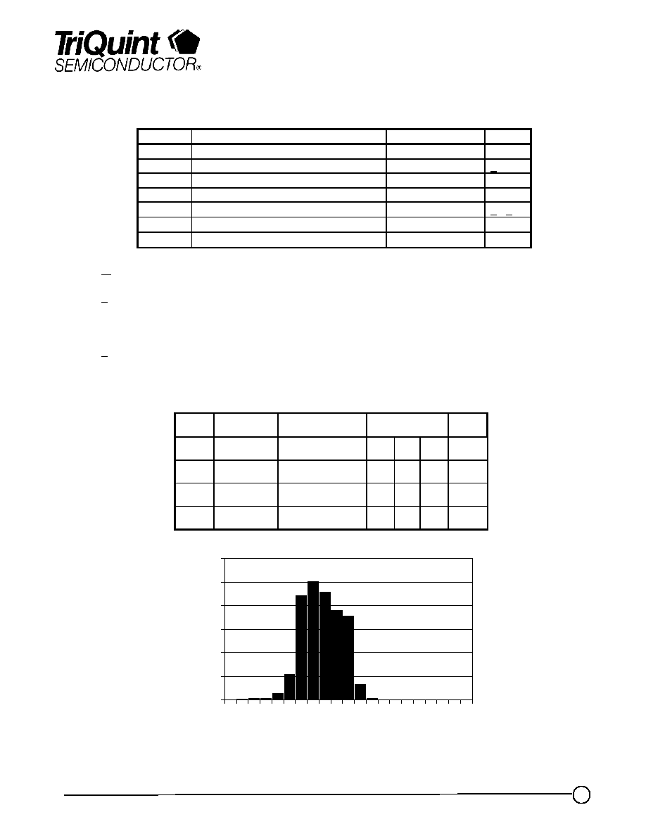
ON-WAFER RF PROBE CHARACTERISTICS
(T
A
= 25
°C ± 5°C)
Symbol Parameter
Test Condition
Vctnl=0V / -2.5V
Limit
Min Nom Max
Units
IL
Insertion Loss F = 18, 19, 20 GHz
States 0 and 31
-5.5
-4.6
-4.0
dB
IRL
Input Return
Loss
F = 18, 19, 20 GHz
States 0 and 31
-16
-11
dB
ORL
Output Return
Loss
F = 18, 19, 20 GHz
States 0 and 31
-14
-11
dB
PS
Phase Shift
F = 18, 19, 20 GHz
State 31
342
344
350
deg
0
200
400
600
800
1000
1200
-5.0 -4.9 -4.8 -4.7 -4.6 -4.5 -4.4 -4.3 -4.2 -4.1 -4.0
19 GHz Reference State Insertion Loss (dB)
Nu
mb
er
o
f
Devic
e
s
TGC1439A
TriQuint Semiconductor Texas : (972)994 8465 Fax (972)994 8504 Web: www.triquint.com
3
Advance Product Information
May 3, 2000
Note: Devices designated as EPU are typically early in their characterization process prior to finalizing all electrical and process
specifications. Specifications are subject to change without notice.
Typical Fixtured Performance Over the 18-20 GHz Band
0
200
400
600
800
1000
1200
1400
-5.0 -4.9 -4.8 -4.7 -4.6 -4.5 -4.4 -4.3 -4.2 -4.1 -4.0
19 GHz State 31 Phase Shift (deg)
Nu
mb
er
o
f
Devic
e
s
19 GHz State 31 Insertion Loss (dB)
Nu
mb
er
o
f
Devic
e
s
0
100
200
300
400
500
600
700
800
340
341
342
343
344
345
346
347
348
349
350
Parameter
Unit
-5.0 V
-2.5 V
Mean Insertion Loss
dB
-4.9
-5.0
Mean Loss Flatness
dB
0.3
0.6
Peak Amplitude Error
dBpp
1.2
1.3
RMS Amplitude Error
dB
0.25
0.30
Peak Phase Shift Error
deg
-3 / +7
-3 / +7
RMS Phase Shift Error
deg
3.0
2.7
Loss Temp. Variation
dB/
°C
-0.0048
-0.0052
Ave Input Return Loss
dB
-16
-15
Ave Output Return Loss
dB
-15
-15
TGC1439A
TriQuint Semiconductor Texas : (972)994 8465 Fax (972)994 8504 Web: www.triquint.com
4
Advance Product Information
May 3, 2000
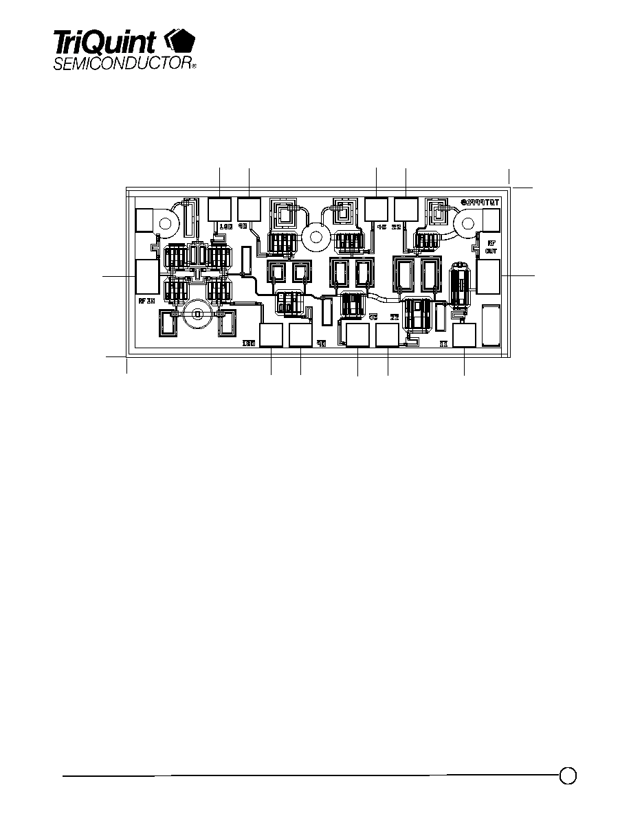
Mechanical Characteristics
Note: Devices designated as EPU are typically early in their characterization process prior to finalizing all electrical and process
specifications. Specifications are subject to change without notice.
Units: millimeters
Thickness: 0.1016
Chip size tolerance: +/- 0.0508
Vcntl = -5.0 V to -2.5 V
Passive device, RF IN and RF OUT designators for reference only
Bond Pad #1
(RF IN)
0.100 x 0.150
Bond Pad #2
(RF OUT)
0.100 x 0.150
Bond Pad #3
(180º Bit ON: V= Vcntl)
0.100 x 0.100
Bond Pad #4
(180º Bit ON: V= 0.0V)
0.100 x 0.100
Bond Pad #5
(90º Bit ON: V= Vcntl)
0.100 x 0.100
Bond Pad #6
(90º Bit ON: V= 0.0V)
0.100 x 0.100
Bond Pad #7
(45º Bit ON: V= Vcntl)
0.100 x 0.100
Bond Pad #8
(45º Bit ON: V= 0.0V)
0.100 x 0.100
Bond Pad #9
(22.5º Bit ON: V= Vcntl)
0.100 x 0.100
Bond Pad #10
(22.5º Bit ON: V= 0.0V)
0.100 x 0.100
Bond Pad #11
(11.25º Bit ON: V= Vcntl)
0.100 x 0.100
0.000
0.
0
0
0
0.354
0.750
1.
69
3
0.
6
3
9
0.354
0.
7
6
9
1.
02
0
1.
15
0
1.
49
0
0.
41
2
0.
54
2
1
.
102
1
.
234
1
2
4
3 5
6
8 10
7 9
11
TGC1439A
TriQuint Semiconductor Texas : (972)994 8465 Fax (972)994 8504 Web: www.triquint.com
5
Advance Product Information
May 3, 2000
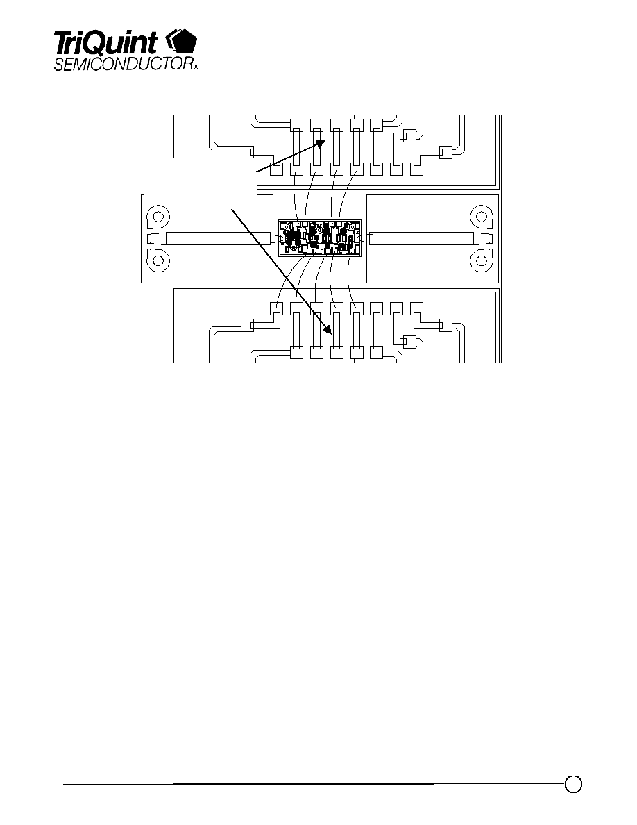
Chip Assembly and Bonding Diagram
Reflow process assembly notes:
·= AuSn (80/20) solder with limited exposure to temperatures at or above 300C
·= alloy station or conveyor furnace with reducing atmosphere
·= no fluxes should be utilized
·= coefficient of thermal expansion matching is critical for long-term reliability
·= storage in dry nitrogen atmosphere
Component placement and adhesive attachment assembly notes:
·= vacuum pencils and/or vacuum collets preferred method of pick up
·= avoidance of air bridges during placement
·= force impact critical during auto placement
·= organic attachment can be used in low-power applications
·= curing should be done in a convection oven; proper exhaust is a safety concern
·= microwave or radiant curing should not be used because of differential heating
·= coefficient of thermal expansion matching is critical
Interconnect process assembly notes:
·= thermosonic ball bonding is the preferred interconnect technique
·= force, time, and ultrasonics are critical parameters
·= aluminum wire should not be used
·= discrete FET devices with small pad sizes should be bonded with 0.0007-inch wire
·= maximum stage temperature: 200C
GaAs MMIC devices are susceptible to damage from Electrostatic Discharge. Proper precautions should
be observed during handling, assembly and test.
Recommend 500
series resistance
on the control lines
TGC1439A