Äîêóìåíòàöèÿ è îïèñàíèÿ www.docs.chipfind.ru
TriQuint Semiconductor Texas : (972)994 8465 Fax (972)994 8504 Web: www.triquint.com
Advance Product Information
1
0.3 - 10 GHz Downconverter TGC1411-EPU
Key Features and Performance
·
0.25um pHEMT Technology
·
0.3-10 GHz RF/LO Frequency Range
·
0.15-2.5 GHz IF Frequency Range
·
Nominal Conversion Gain of 12 dB
·
Bias 3-5V @ 26 mA
·
Chip Dimensions 1.8 mm x 2.6mm
Primary Applications
·
Satellite Systems
·
Point-to-Point Radio
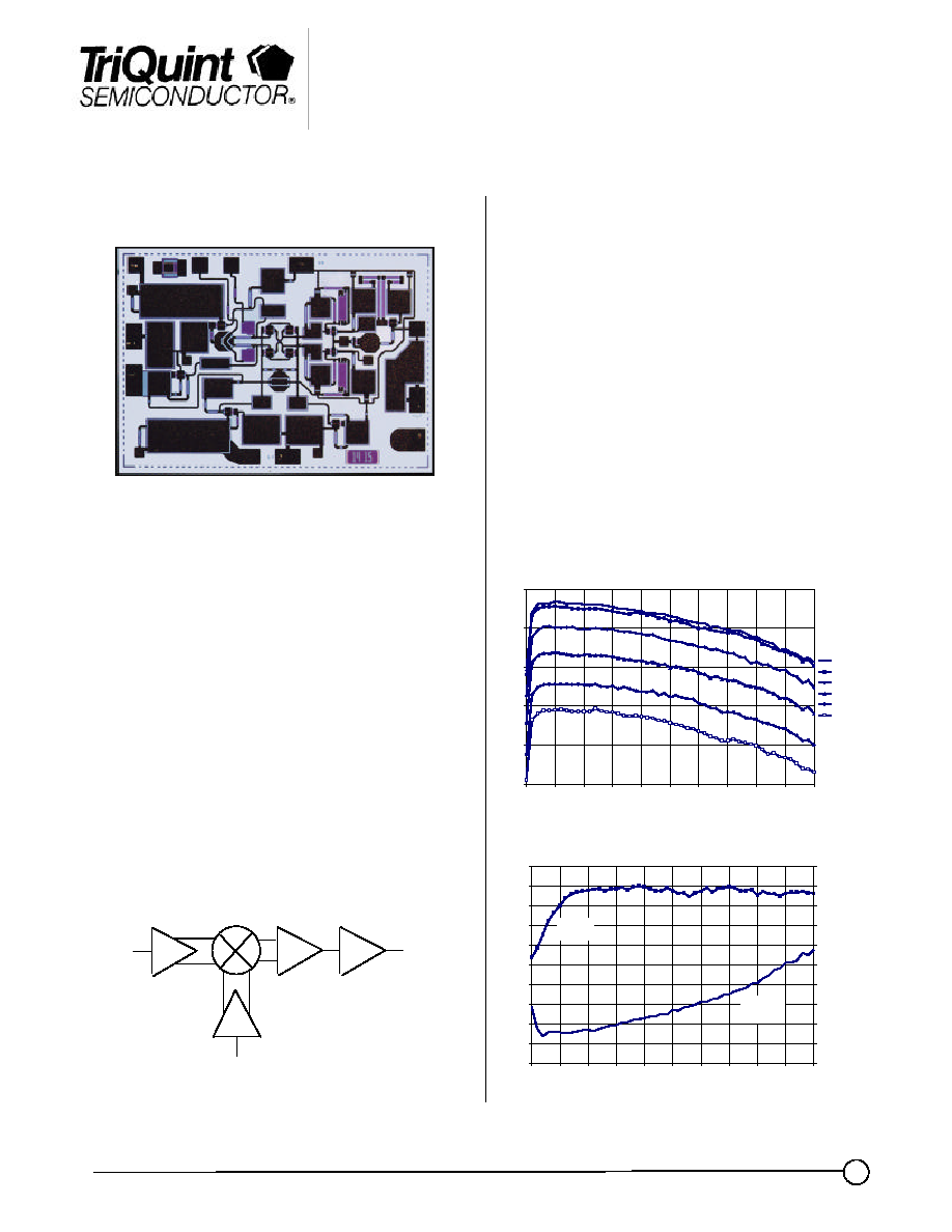
The TriQuint TGC1411-EPU is a double balanced
MMIC mixer design using TriQuint's proven 0.25 um
Power pHEMT process to support a variety of
communication system applications including satellite.
The double balanced design consists of an integrated
Gilbert cell mixer core, RF/LO baluns, differential
combiner, and output driver amplifier. The TGC1411
may be operated from a single +3 V to +5 V power
supply with typical current draw of 26 mA. The
nominal LO power requirement is -5 dBm. The
TGC1411 may also be operated as an up-converter.
The TGC1411 requires a minimum of off-chip
components employing only a 100 pF off-chip bypass
capacitor for the power supply line. No additional off-
chip RF matching components are required. Each
device is 100% DC and RF tested on-wafer to ensure
performance compliance. The device is available in
chip form.
Note: Devices designated as EPU are typically early in their characterization process prior to finalizing all electrical and process
specifications. Specifications are subject to change without notice.
RF
IN
LO
IN
IF
OUT
TGA1411 Typical Down-Conversion Gain
LSB, +5.0V, LO = -5dBm, +25C
3
6
9
12
15
18
0.1
1.1
2.1
3.1
4.1
5.1
6.1
7.1
8.1
9.1
10.1
RF Frequency (GHz)
Conversion Gain (dB)
IF=151MHz
IF=501MHz
IF=1001MHz
IF=1501MHz
IF=2001MHz
IF=2501MHz
TGC 1411
TGA1411 Typical P1dB and SSB Noise Figure
LSB, +5.0V, LO = -5dBm, +25C
-9
-8
-7
-6
-5
-4
-3
-2
-1
0
1
0.1
1.1
2.1
3.1
4.1
5.1
6.1
7.1
8.1
9.1
10.1
RF Frequency (GHz)
Output P1dB (dBm)
8
9
10
11
12
13
14
15
16
17
18
SSB Noise Figure (dB)
Noise
Figure
P1dB
TGC 1411
TriQuint Semiconductor Texas : (972)994 8465 Fax (972)994 8504 Web: www.triquint.com
Advance Product Information
2
RECOMMENDED MAXIMUM RATINGS
Symbol
Parameter
Value
Notes
V
+
Positive Supply Voltage
8 V
I
+
Positive Supply Current
80 mA
3/
P
D
Power Dissipation
0.64 W
P
IN
Input Continuous Wave Power
14 dBm
T
CH
Operating Channel Temperature
150
°
C
1/, 2/
T
M
Mounting Temperature (30 seconds)
320
°
C
T
STG
Storage Temperature
-65
°
C to 150
°
C
1/
These ratings apply to each individual FET
2/
Junction operating temperature will directly affect the device mean time to failure
(MTTF). For maximum life it is recommended that junction temperatures be
maintained at the lowest possible levels.
3/
Total current for the entire MMIC
Electrical Characteristics
Note: Devices designated as EPU are typically early in their characterization process prior to finalizing all electrical and process
specifications. Specifications are subject to change without notice.
DC PROBE TESTS
(T
A
= 25
°
C
±
5
°
C)
Symbol
Parameter
Minimum
Maximum
Value
V
P
Test FET
Pinch-off Voltage
-1.5
-0.5
V
BV
Test FET
Breakdown Voltage gate-source
-30
-8
V
BV
Test FET
Breakdown Voltage gate-drain
-30
-8
V
ON-WAFER RF PROBE CHARACTERISTICS
(T
A
= 25
°
C
±
5
°
C)
Symbol Parameter
Test Condition
Vd=5V, LO=-5dBm
Limit
Min Nom Max
Units
G
Conversion
Gain
F
RF
= 1.0 GHz
F
LO
= 1.6 GHz
13
16
20
dB
dB
ILO
LO Isolation
F
LO
= 1.6 GHz
-
-30
-20
dB
P1dB
Output P1dB
F
RF
= 1.0 GHz
F
LO
= 1.6 GHz
-5
-1
-
dBm
IDC
DC Current
-
26
35
mA
TriQuint Semiconductor Texas : (972)994 8465 Fax (972)994 8504 Web: www.triquint.com
Advance Product Information
3
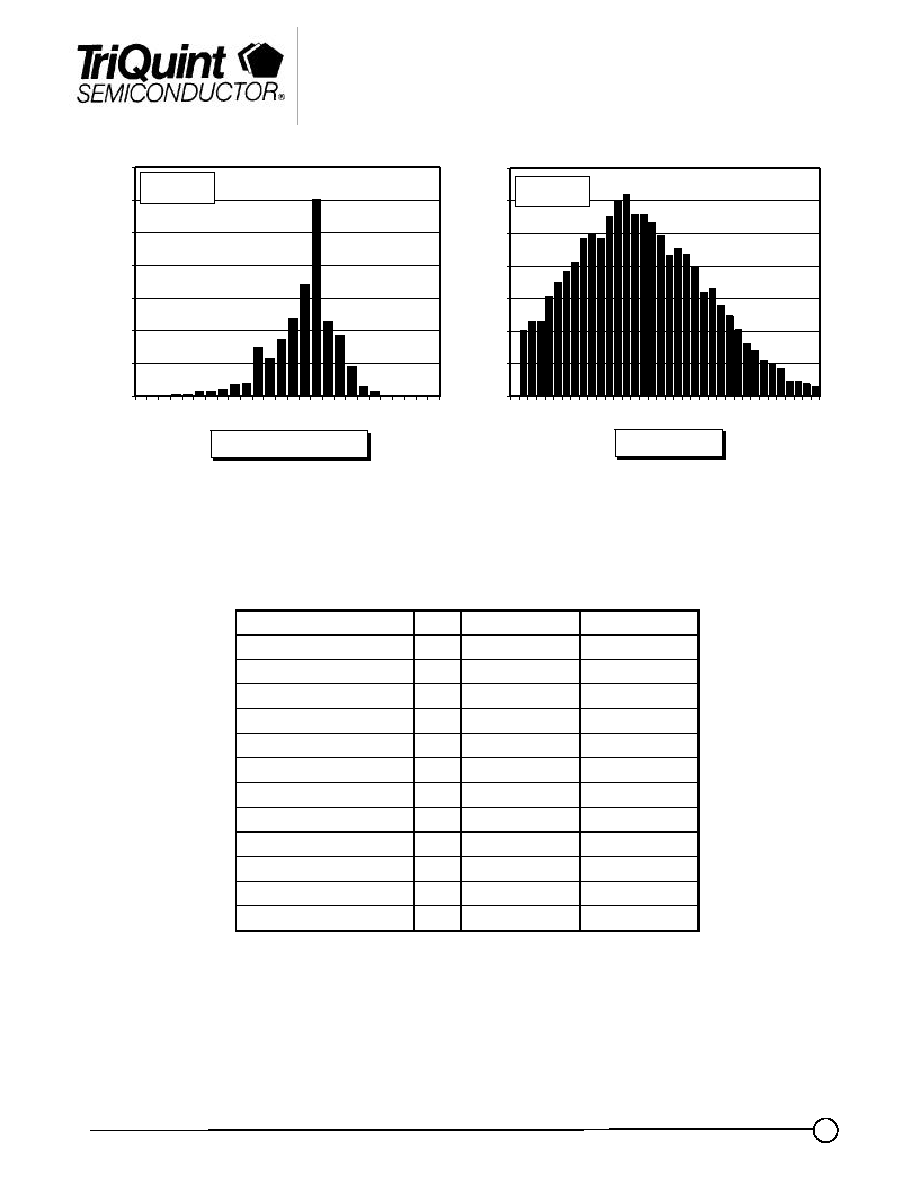
0
500
1000
1500
2000
2500
3000
3500
14
15
16
17
18
19
Number of Devices
Mean = 16.7 dB
Sigma = 0.54 dB
RF-Probe Performance Summary
LO-IF Isolation
LO-IF Isolation
Down-Conversion Gain
Down-Conversion Gain
Note: Devices designated as EPU are typically early in their characterization process prior to finalizing all electrical and process
specifications. Specifications are subject to change without notice.
0
100
200
300
400
500
600
700
15
20
25
30
35
40
45
50
LO to Output Isolation (dB)
Number of Devices
Mean = 29.3 dB
Sigma = 7.7 dB
Typical Performance
Parameter
Units
+5V Supply
+3V Supply
RF Frequency
GHz
0.3 - 10.0
0.3 - 10.0
IF Frequency
GHz
0.15 - 2.5
0.15 - 2.5
LO Frequency
GHz
0.45 - 12.5
0.45 - 12.5
LO Power
dBm
-5
0
-5
0
Conversion Gain*
dB
15
17.0
13
14.5
Output P
1dB
*
dBm
-1
0.0
-8
-4.5
SSB Noise Figure*
dB
11
15.0
11
11.0
LO Isolation
dB
-30
-30
Input Port Return Loss
dB
-12
-12
Output Port Return Loss
dB
-12
-12
LO Port Return Loss
dB
-12
-12
Supply Current
mA
26
28.0
22
24.0
* IF = 501 MHz
TriQuint Semiconductor Texas : (972)994 8465 Fax (972)994 8504 Web: www.triquint.com
Advance Product Information
4
Mechanical Characteristics
Note: Devices designated as EPU are typically early in their characterization process prior to finalizing all electrical and process
specifications. Specifications are subject to change without notice.
TriQuint Semiconductor Texas : (972)994 8465 Fax (972)994 8504 Web: www.triquint.com
Advance Product Information
5
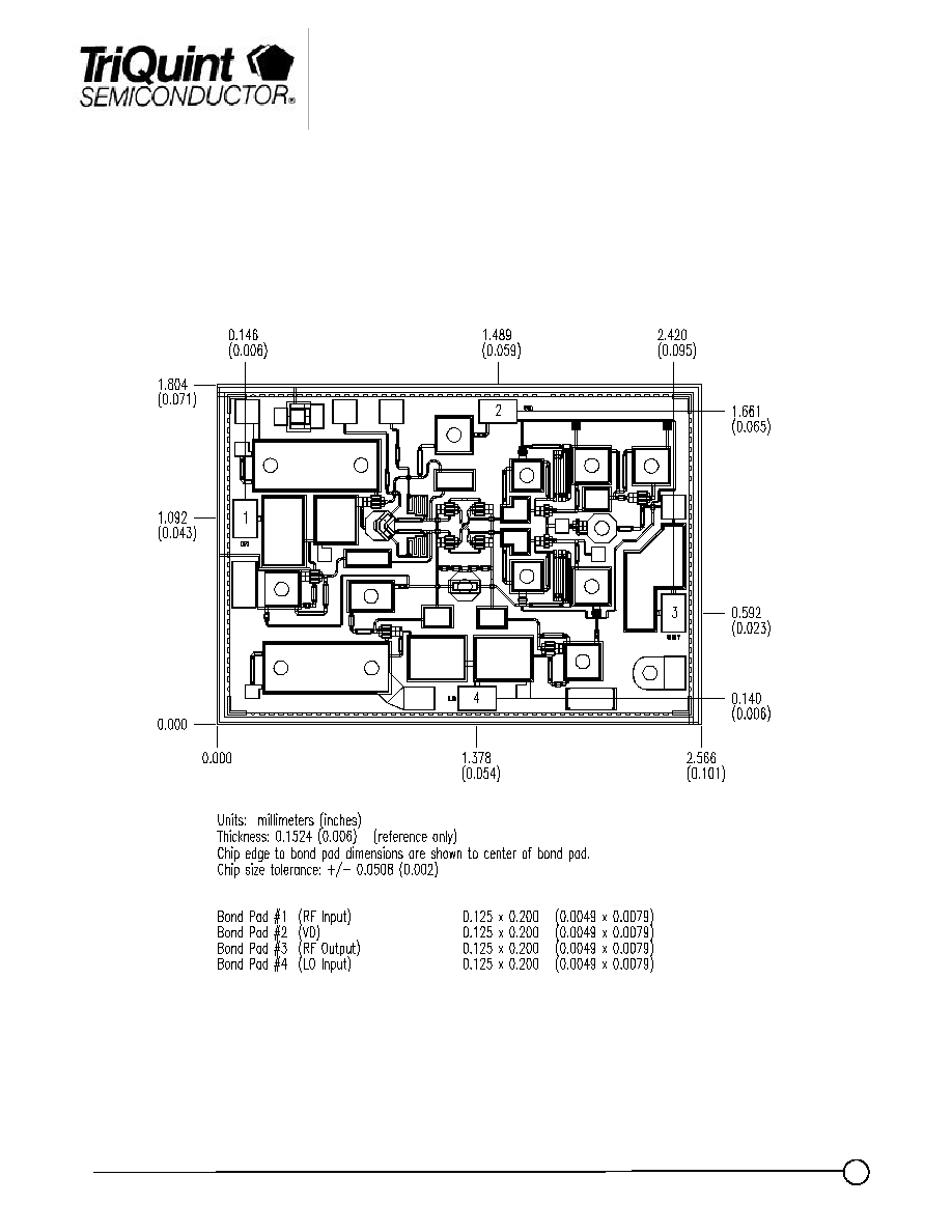
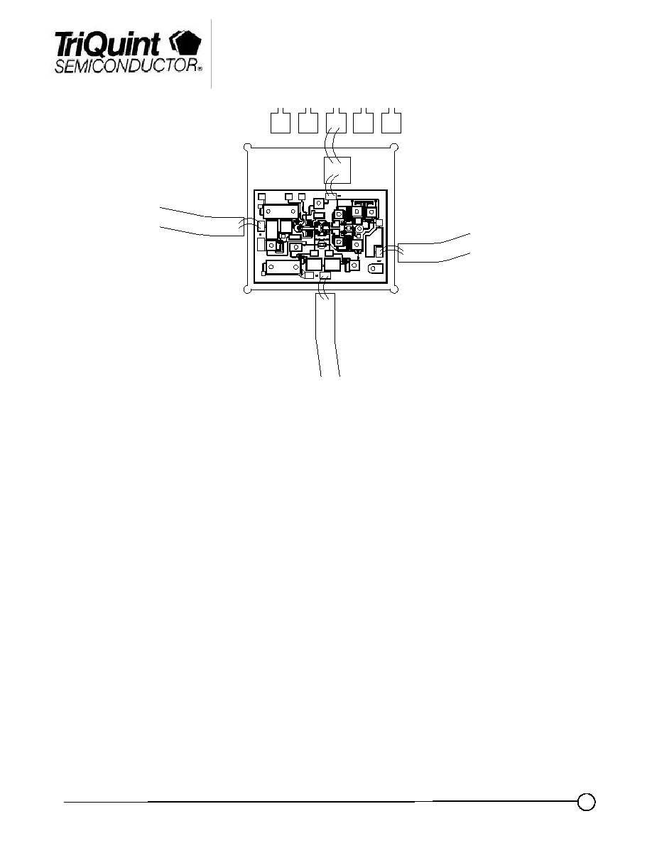
Chip Assembly and Bonding Diagram
Reflow process assembly notes:
·
AuSn (80/20) solder with limited exposure to temperatures at or above 300
C
·
alloy station or conveyor furnace with reducing atmosphere
·
no fluxes should be utilized
·
coefficient of thermal expansion matching is critical for long-term reliability
·
storage in dry nitrogen atmosphere
Component placement and adhesive attachment assembly notes:
·
vacuum pencils and/or vacuum collets preferred method of pick up
·
avoidance of air bridges during placement
·
force impact critical during auto placement
·
organic attachment can be used in low-power applications
·
curing should be done in a convection oven; proper exhaust is a safety concern
·
microwave or radiant curing should not be used because of differential heating
·
coefficient of thermal expansion matching is critical
Interconnect process assembly notes:
·
thermosonic ball bonding is the preferred interconnect technique
·
force, time, and ultrasonics are critical parameters
·
aluminum wire should not be used
·
discrete FET devices with small pad sizes should be bonded with 0.0007-inch wire
·
maximum stage temperature: 200
C
GaAs MMIC devices are susceptible to damage from Electrostatic Discharge. Proper precautions should
be observed during handling, assembly and test.
RF
IN
IF
OUT
VD
100 pF
LO
IN