
TriQuint Semiconductor Texas : (972)994 8465 Fax (972)994 8504 Web: www.triquint.com
Product Datasheet
1
1
23 - 29 GHz High Power Amplifier TGA9070-SCC
Key Features and Performance
·
0.25um pHEMT Technology
·
23 GHz - 29 GHz Frequency Range
·
Nominal 1 Watt (28GHz) @ P1dB
·
Nominal Gain of 23 dB
·
Bias 7V @ 400 mA
·
Chip Dimensions 4.1mm x 3.0mm
Primary Applications
·
LMDS
·
Point-to-Point Radio
Description
The TriQuint TGA9070-SCC is a three stage
HPA MMIC design using TriQuint's proven
0.25 um Power pHEMT process to support
a variety of millimeter wave applications
including point-to-point digital radio, LMDS/LMCS
and Ka-band satellite spacecraft and ground
terminals.
The three stage design consists of a 400 um input
device driving a pair of 600 um interstage devices
followed by four 600 um output devices.
The TGA9070 provides greater than 1W of
output power across 23-29 GHz with a typical
PAE of 35%. Typical small signal gain is 23 dB.
The TGA9070 requires minimum off-chip
components. Each device is 100% DC and RF
tested on-wafer to ensure performance compliance.
The device is available in chip form.
TriQuint Semiconductor Texas : (972)994 8465 Fax (972)994 8504 Web: www.triquint.com
Product Datasheet
2
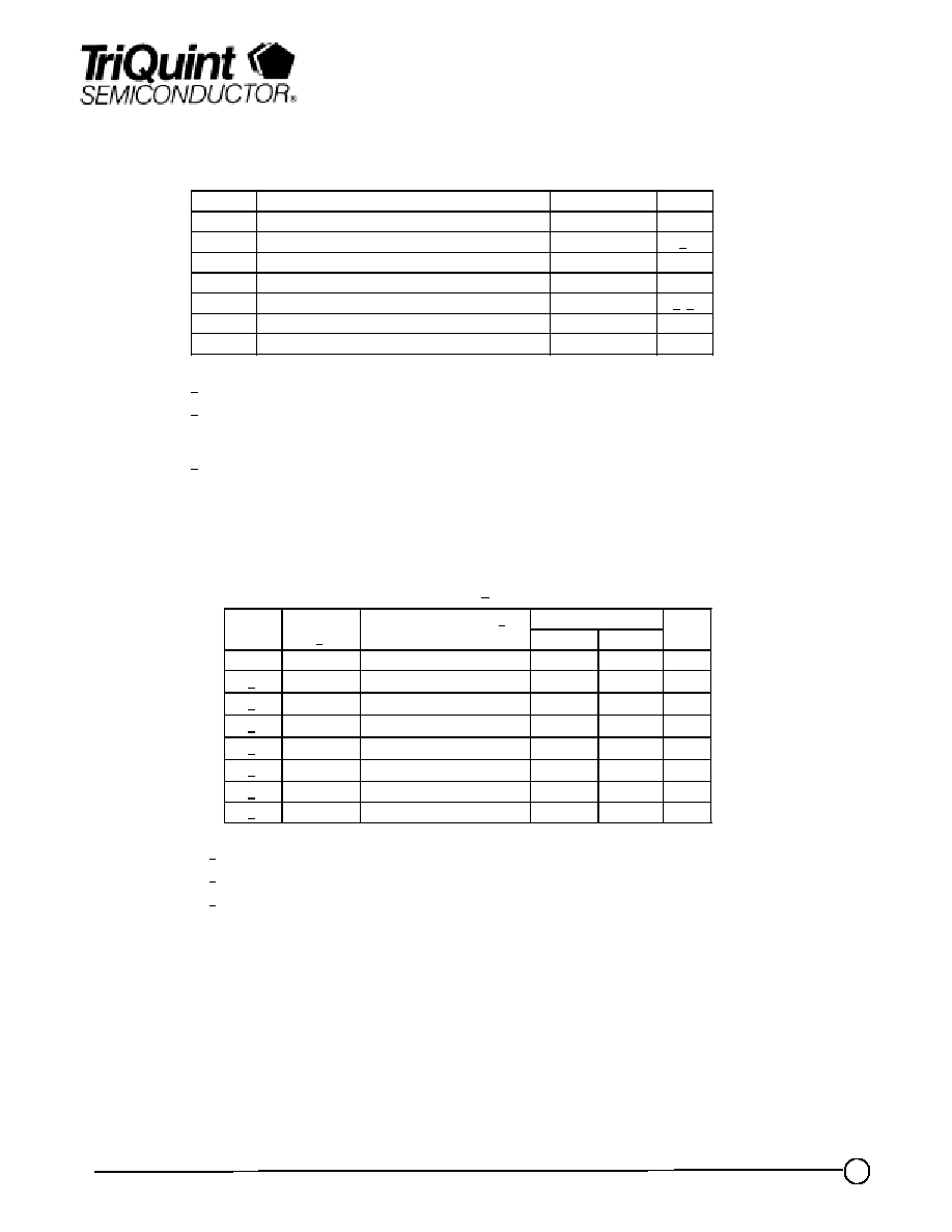
TABLE I
RECOMMENDED MAXIMUM RATINGS
SYMBOL
PARAMETER
VALUE
NOTES
V
+
POSITIVE SUPPLY VOLTAGE
8 V
I
+
POSITIVE SUPPLY CURRENT
1 A
1/
P
D
POWER DISSIPATION
8 W
P
IN
INPUT CONTINUOUS WAVE POWER
20dBm
T
CH
OPERATING CHANNEL TEMPERATURE
150
0
C
2/ 3/
T
M
MOUNTING TEMPERATURE (30 SECONDS)
320
0
C
T
STG
STORAGE TEMPERATURE
-65 to 150
0
C
1/
Total current for all 3 stages
2/
Junction operating temperature will directly affect the device mean time to failure (MTTF). For
maximum life, it is recommended that junction temperatures be maintained at the lowest
possible levels.
3/
These ratings apply to each individual FET
TABLE II
DC PROBE TESTS (100%)
(T
A
= 25
°
C + 5
°
C)
NOTES
SYMBOL
TEST CONDITIONS 3/
LIMITS
UNITS
2/
MIN
MAX
I
DSS1
STD
40
188
mA
1/
|V
P1
|
STD
0.5
1.5
V
1/
|V
P2
|
STD
0.5
1.5
V
1/
|V
P3
|
STD
0.5
1.5
V
1/
|V
P4
|
STD
0.5
1.5
V
1/
|V
P5
|
STD
0.5
1.5
V
1/
|V
BVGD1-5
|
STD
12
30
V
1/
|V
BVGS1
|
STD
12
30
V
1/
V
P
, V
BVGD
, and V
BVGS
are negative
2/
Subscripts are referred to Q1, Q2, Q3, Q4, Q5 accordingly.
3/
The measurement conditions are subject to change at the manufacture's discretion (with
appropriate notification to the buyer).
STD Standard Test Conditions (see Table III for definitions)

TriQuint Semiconductor Texas : (972)994 8465 Fax (972)994 8504 Web: www.triquint.com
Product Datasheet
3
TABLE IV
ELECTRICAL CHARACTERISTICS
(T
A
= 25
°
C + 5
°
C)
V
d
= 6V, I
d
= 400 mA
NOTE
TEST
MEASUREMENT
CONDITIONS
VALUE
UNITS
1/
MIN
TYP
MAX
2/
POWER OUTPUT
AT 1 dB GAIN
COMPRESSION
F = 23 - 27 GHz
F = 28 GHz
F = 29 GHz
28.5
29
28.5
30
30.5
30
dBm
dBm
dBm
POWER ADDED
EFFICIENCY
F = 23 29 GHz
35
%
SMALL-SIGNAL
GAIN MAGNITUDE
F = 23 GHz
F = 24 28 GHz
F = 29 GHz
19
20
19
21
23
21
26
28
26
dB
dB
dB
INPUT RETURN LOSS
MAGNITUDE
F = 23 - 29 GHz
-10
dB
OUTPUT RETURN
LOSS MAGNITUDE
F = 23 29 GHz
-10
dB
1/ RF Probe data is taken at 1 GHz steps
2/
P/
T typically 0.02dB/
°
C
TABLE V
RELIABILITY DATA
PARAMETER
BIAS CONDITIONS
P
DISS
R
JC
T
CH
MTTF
V
D
(V)
I
D
(mA)
(W)
(C/W)
(
°
C)
(HRS)
6
400
2.4
22.08
123
> 2 E6
R
JC
Thermal resistance
(channel to backside)
7
400
2.8
22.5
133
> 1 E6
Note: Assumes eutectic attach using 80/20 AuSn mounted to a 10mil CuMo Carrier at 70
°
C baseplate
temperature. Worst case condition with no RF applied, 100% of DC power is dissipated.

TriQuint Semiconductor Texas : (972)994 8465 Fax (972)994 8504 Web: www.triquint.com
Product Datasheet
4
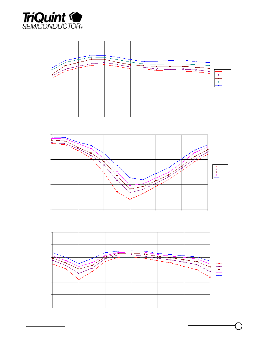
Statistical Performance Summary
2 4
2 6
2 8
3 0
3 2
3 4
2 3
2 4
2 5
2 6
2 7
2 8
2 9
F re q u e n c y (G H z )
O
u
t
p
u
t
P
o
w
e
r @
1d
B
C
o
m
p
ressi
o
n
(
d
Bm
)
5 th
2 5th
5 0th
7 5th
9 5th
0
10
20
30
40
50
23
24
25
26
2 7
2 8
2 9
Fr e que n cy (G H z )
PA
E (
%
)
5t h
25 th
50 th
75 th
95 th
TriQuint Semiconductor Texas : (972)994 8465 Fax (972)994 8504 Web: www.triquint.com
Product Datasheet
5
- 2 4
- 2 0
- 1 6
- 1 2
- 8
- 4
0
2 3
2 4
2 5
2 6
2 7
2 8
2 9
F r e q u e n c y ( G H z )
In
p
u
t
R
e
t
u
r
n
L
o
s
s
(
d
B
)
5 t h
2 5 t h
5 0 t h
7 5 t h
9 5 t h
1 0
1 4
1 8
2 2
2 6
3 0
2 3
2 4
2 5
2 6
2 7
2 8
2 9
F r e q u e n c y (G H z )
G
a
in
(
d
B
)
5t h
25 th
50 th
75 th
95 th
- 2 4
- 2 0
- 1 6
- 1 2
- 8
- 4
0
2 3
2 4
2 5
2 6
2 7
2 8
2 9
F r e q u e n c y ( G H z )
O
u
t
put
R
e
t
u
r
n
Los
s
(
d
B
)
5 t h
2 5 t h
5 0 t h
7 5 t h
9 5 t h
Statistical Performance Summary