Product Data Sheet
1
TriQuint Semiconductor Texas Phone: (972)994 8465 Fax: (972)994 8504 Web: www.triquint.com
2 - 18 GHz Low Noise Amplifier TGA8344-SCC
Key Features and Performance
·
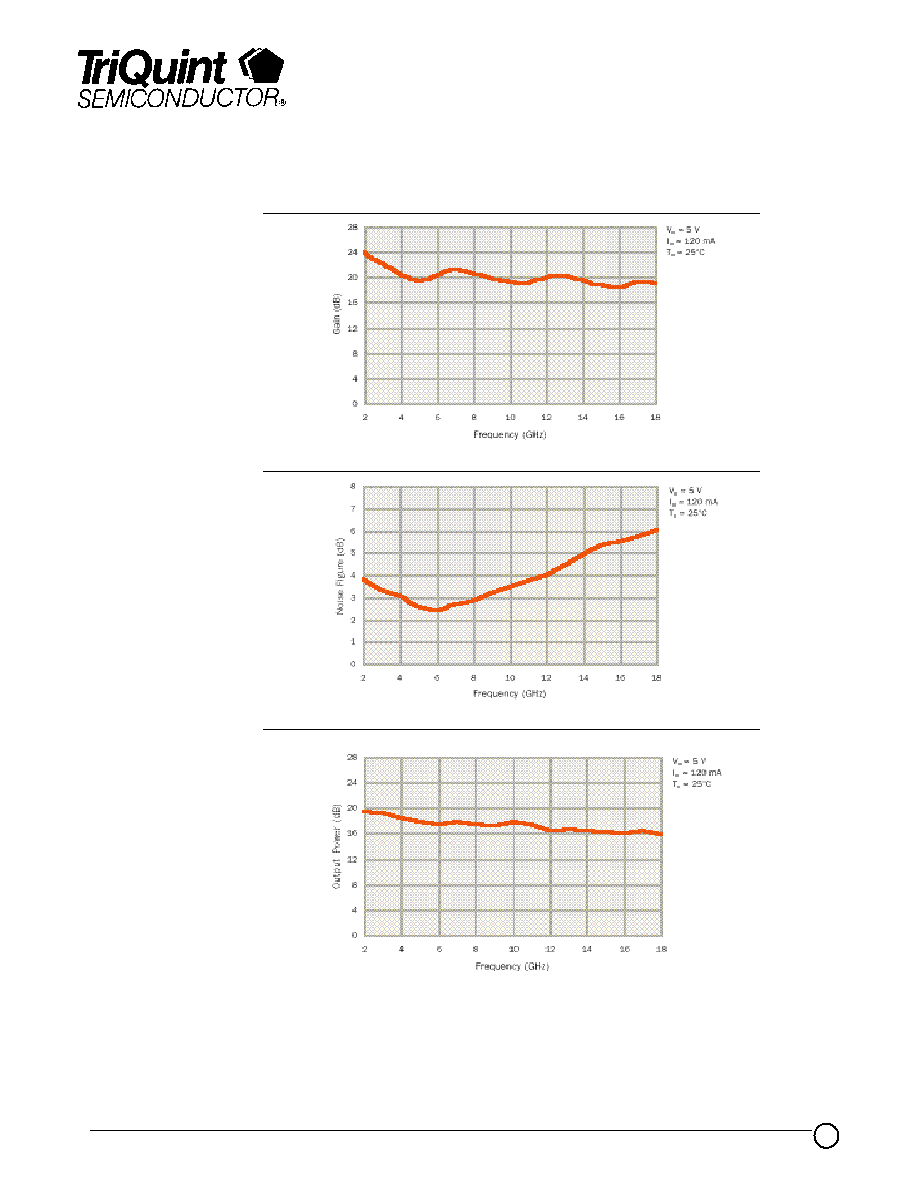
2 to 18 GHz Frequency Range
·
Typical 4 dB Noise Figure at Midband
·
16 dBm Typical Output Power at 1 dB
Gain Compression
·
19 dB Typical Gain
·
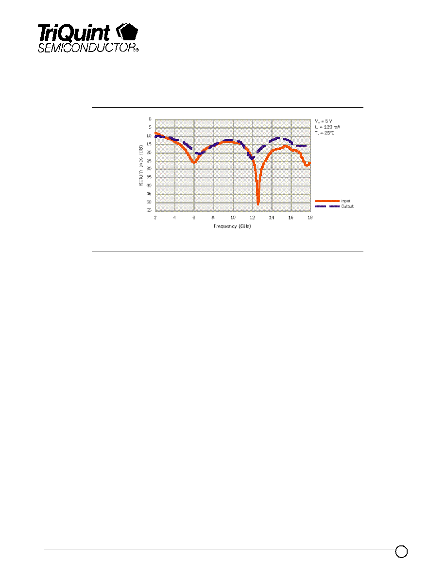
Typical Input SWR 1.5:1 and Output
SWR 1.6:1
·
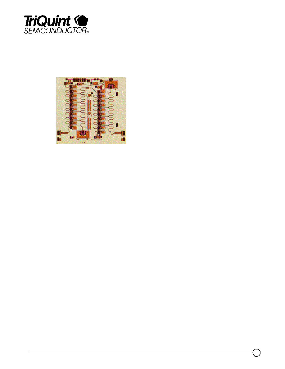
3.9878 x 3.810 x 0.1016 mm (0.1570
0.150 x 0.0040 in.)
Description
The TriQuint TGA8344-SCC features two cascaded monolithic low-noise distributed
amplifiers with on-chip bias operating from 2 to 18 GHz. This die offers the
advantage of high gain, typically 19 dB, in compact die size with simplified biasing
configuration. Noise figure is typically 4 dB. The two cascade amplifiers have
eighteen 122 um gatewidth FETs providing 16 dBm of output power at 1 dB gain
compression. Input return loss is typically 14 dB from 2 to 18 GHz and output return
loss is typically 13 dB. Ground is provided to the circuitry through vias to the
backside metallization. The TGA8344-SCC small size and high gain make it
suitable for use in a variety of wide-band electronic commercial and warfare
systems.
Bond pad and backside metallization is gold plated for compatibility with eutectic
alloy attachment methods as well as the thermocompression wire-bonding
processes. The TGA8344-SCC is supplied in chip form and is readily assembled
using automated equipment.
April 3, 2003
Product Data Sheet
4
TriQuint Semiconductor Texas Phone: (972)994 8465 Fax: (972)994 8504 Web: www.triquint.com
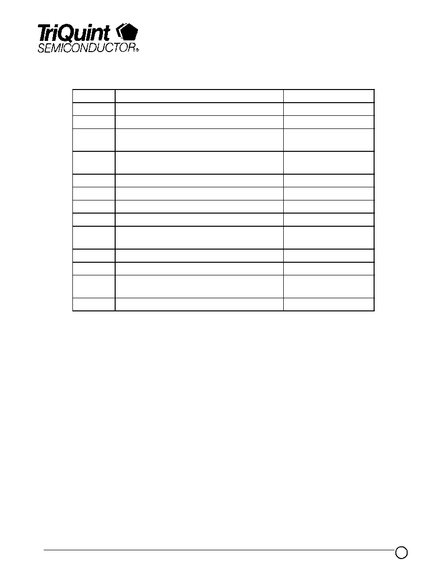
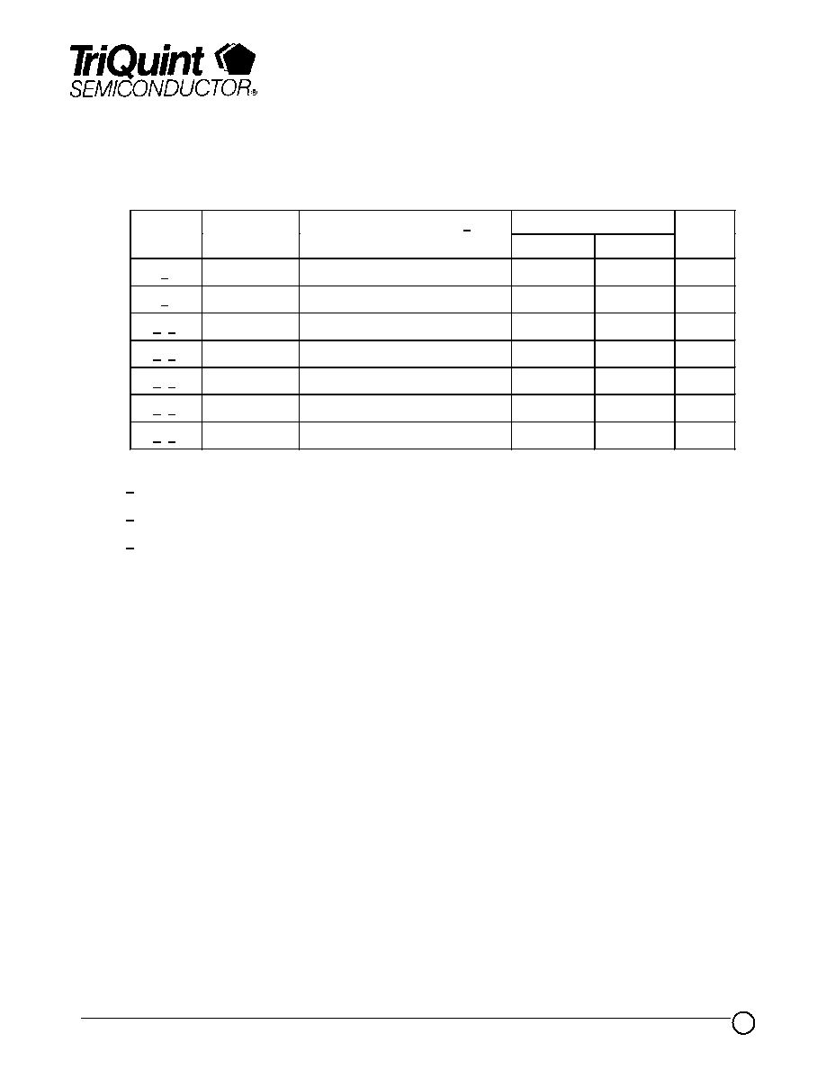
TABLE I
MAXIMUM RATINGS
SYMBOL
PARAMETER
VALUE
V
D
DRAIN SUPPLY VOLTAGE
9V
V
+
POSITIVE SUPPLY VOLTAGE
12V
V
+
- V
-
POSITIVE SUPPLY VOLTAGE RANGE WITH
RESPECT TO NEGATIVE SUPPLY VOLTAGE
0V to 13V
V
CTRL
- V
+
POSITIVE SUPPLY VOLTAGE WITH RESPECT
TO GAIN CONTROL VOLTAGE
0V to 13V
V
-
NEGATIVE SUPPLY VOLTAGE RANGE
5V to 0V
V
CTRL
GAIN CONTROL VOLTAGE RANGE
-5V to 4V
I
+
POSITIVE SUPPLY CURRENT
376mA
I
-
NEGATIVE SUPPLY CURRENT
-8.73mA
P
D
POWER DISSIPATION, AT (OR BELOW) 25
°
C
BASE-PLATE TEMPERATURE
*
5.3W
P
IN
INPUT CONTINUOUS WAVE POWER
23dBm
T
CH
**
OPERATING CHANNEL TEMPERATURE
150
0
C
T
M
MOUNTING TEMPERATURE
(30 SECONDS)
320
0
C
T
STG
STORAGE TEMPERATURE
-65 to 150
0
C
Ratings over channel temperature range, T
CH
(unless otherwise noted)
Stresses beyond those listed under "Maximum Ratings" may cause permanent damage to the
device.
These are stress ratings only, and functional operation of the device at these or any other
conditions beyond those indicated under "RF Specifications" is not implied. Exposure to maximum
rated conditions for extended periods may affect device reliability.
*For operation above 25
°
C base-plate temperature, derate linearly at the rate of 11.2mW/
°
C.
** Operating channel temperature, T
CH
, directly affects the device MTTF. For maximum life, it is
recommended that channel temperature be maintained at the lowest possible level.
TGA8344-SCC
Product Data Sheet
5
TriQuint Semiconductor Texas Phone: (972)994 8465 Fax: (972)994 8504 Web: www.triquint.com
TGA8344-SCC
TABLE II
DC PROBE TESTS (100%)
(T
A
= 25
°
C Nominal)
NOTES
SYMBOL
TEST CONDITIONS 3/
LIMITS
UNITS
MIN
MAX
2/
I
DSS1-9
STD
110
307
mA
2/
G
M1-9
STD
186
340
mS
1/,2/
|V
BVGS1-9
|
STD
6
30
V
1/,2/
|V
P1-9, 1
|
STD
0.5
1.8
V
1/,2/
|V
P1-9, 2
|
STD
0.5
1.8
V
1/,2/
|V
P10-18, 1
|
STD
0.5
1.8
V
1/,2/
|V
P10-18, 2
|
STD
0.5
1.8
V
1/
V
BVGS1-9,
V
P1-9
, and V
P10-18
are negative
2/
Subscripts are referred to Q1 through Q18 accordingly.
3/
The measurement conditions are subject to change at the manufacture's discretion (with
appropriate notification to the buyer).
STD Standard Test Conditions (see Table IV for definitions)