TriQuint Semiconductor Texas Phone: (972)994 8465 Fax: (972)994 8504 Web: www.triquint.com
Product Data Sheet
1
2 - 20 GHz Power Amplifier TGA8334-SCC
Key Features and Performance
·
2 to 20 GHz Frequency Range
·
0.4-W Output Power at 1 dB Gain
Compression at Midband
·
Positive Gain Slope Across Frequency
·
On-Chip Input DC-Blocking Capacitor
·
1.8:1 Input SWR at Midband, 1.3:1
Output SWR at Midband
·
8 dB Gain with +/- 1 dB Flatness
·
3.1750 x 1.8034 x 0.1524 mm (0.125 x
0.071 x 0.006 in.)
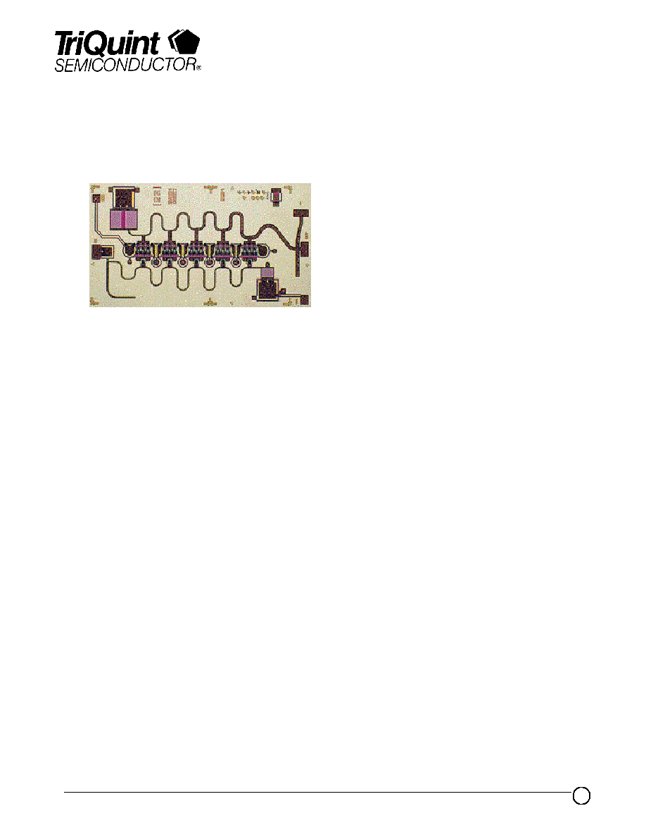
Description
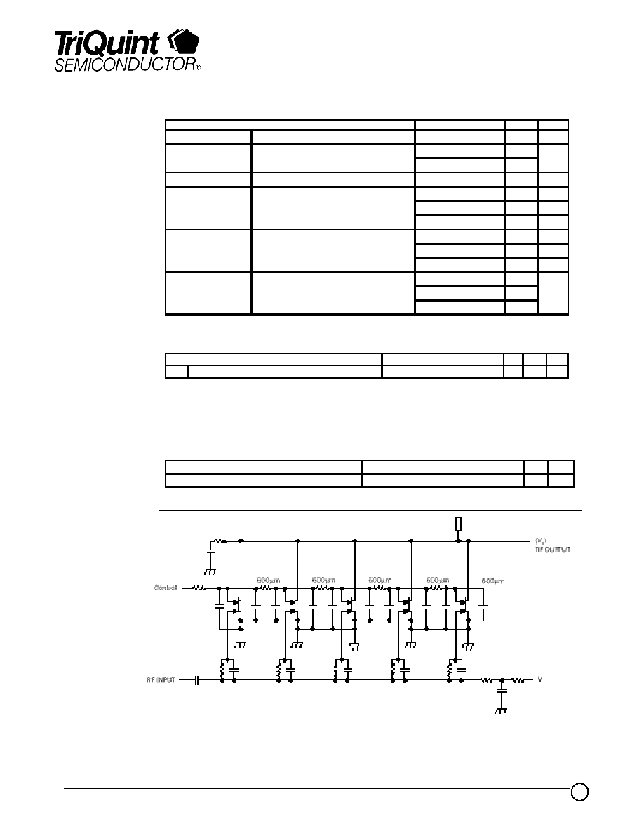
The TriQuint TGA8334-SCC is a GaAs monolithic dual-gate distributed amplifier.
Small-signal gain is typically 8 dB with positive gain slope across the band. Input
and output return loss is typically greater than 9.7 dB. Five 600um gatewidth FETs
provide more than 26 dB output power at 1 dB gain compression at midband.
Ground is provided to the circuitry through vias to the backside metallization.
The TGA8334-SCC is directly cascadable with other broadband TriQuint GaAs
amplifiers, such as the TGA8300-SCC, TGA8622-SCC, and TGA8220-SCC. This
general power amplifier is suitable for a variety or wide-band applications such as
distributed networks, logging stages and oscillator buffers.
Bond pad and backside metallization is gold plated for compatibility with eutectic
alloy attachment methods as well as the thermocompression and thermosonic wire
bonding processes. The TGA8334-SCC is supplied in chip form and is readily
assembled using automated equipment.
TriQuint Semiconductor Texas Phone: (972)994 8465 Fax: (972)994 8504 Web: www.triquint.com
Product Data Sheet
3
TGA8334-SCC
ABSOLUTE
MAXIMUM
RATINGS
Positive supply voltage, V+................................................................................................9 V
Positive supply current, I+..................................................................................................I
DSS
Negative supply voltage range, V-.......................................................................................-5 V to 0 V
Gain control voltage range, V
CTRL
.......................................................................................-5 V to 4 V
Gain control voltage range w ith respect to positive supply voltage, V
CT RL
................................... 0 V to -10 V
Pow er dissipation, P
D
, at (or below ) 25
o
C base-plate temperature *......................................... 7.2 W
Input continuous w ave pow er, P
IN
..................................................................................
27 dBm
Operating Channel temperature, T
CH
**.............................................................................. 150
o
C
Mounting temperature (30 sec.), T
M
.................................................................................. 320
o
C
Storage temperature range, T
STG
...................................................................................... -65 to 150
o
C
Ratings over operating channel tem perature range, TCH (unless otherw ise noted).
Stresses beyond those listed under "Absolute Maximum Ratings" may cause permanent damage to the device.
These are stress ratings only, and functional operation of the device at these or any other conditions beyond
those indicated under "RF Characteristics" is not implied. Exposure to absolute maximum rated conditions
for extended periods may affect device reliability.
* For operation above 25
o
C base-plate temperature, derate linearly at the rate of 15.2 mW/
o
C.
** Operating channel temperature directly affects the device MTTF. For maximum life, it is recommended that
channel temperature be maintained at the low est possible level. These ratings apply to each individual FET.
TriQuint Semiconductor Texas Phone: (972)994 8465 Fax: (972)994 8504 Web: www.triquint.com
Product Data Sheet
5
TGA8334-SCC
THERMAL
INFORMATION
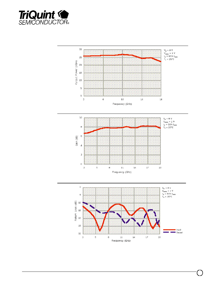
RF CHARACTERISTICS
EQUIVALENT
SCHEMATIC
V
D
= 8 V, V
CNTR
= 1 V, I
D
= 50% I
DSS
, T
A
= 25
o
C,
DC CHARACTERISTICS
P AR AMETER
TEST CONDITION
NOM
UNIT
R
J C
Thermal res is tance (channel to backs ide) V
D
= 8 V, I
D
= 50% I
DS S
, V
CTRL
= 1 V 18.7 °C/W
T
A
= 25
O
C
V
DS
for I
DSS
is the drain voltage between 0.5 V and 3.5 V at which drain current is highest at DC Autoprobe.
P ARAMETER
TES T C ONDITIONS
M IN MAX UNIT
I
DS S
Total zerogate voltage drain curre nt a t s a tura tion V
DS
= 0.5 V to 3.5 V, V
GS
= 0 V 630 1170 mA
P AR AM ETER
TEST C ONDITIONS
TYP
UNIT
G
p
Small-s ignal pow er gain
f = 2 to 20 GHz
8
dB
P
1dB
Output pow er at 1dB gain
f = 2 to 14 GHz
26
dBm
compres s ion
f =14 to 18 GHz
25
G
p
Gain flatnes s
f = 2 to 20 GHz
±1
dB
f = 2 GHz
1.6:1
-
SWR(in)
Input s tanding w ave ratio
f = 9 GHz
1.7:1
-
f =18 GHz
1.1:1
-
f = 2 GHz
2.0:1
-
SWR(out)
Output s tanding w ave ratio
f = 9 GHz
1.4:1
-
f =18 GHz
1.5:1
-
f = 2 GHz
38
IP
3
Output thirdorder intercept point
f = 9 GHz
41
dBm
f =18 GHz
38