
TriQuint Semiconductor Texas Phone: (972)994 8465 Fax: (972)994 8504 Web: www.triquint.com
Product Data Sheet
1
.1 - 3.5 GHz Low Noise Amplifier TGA8061-SCC
Key Features and Performance
ñ
100 MHz to 3.5 GHz Frequency Range
ñ
3 dB Bandwidth Exceeds 5 Octaves
ñ
2.4 dB Noise Figure with Low Input and
Output SWR
ñ
18 dB Gain
ñ
15 dBm Output Power at 1 dB Gain
Compression
ñ
Operates from Single 12V Supply
ñ
1.524 x 1.524 x 0.102 mm (0.060 x 0.060
x 0.004 in.)
Description
The TriQuint TGA8061-SCC is a GaAs monolithic low noise amplifier intended for
use as a universal gain block in applications requiring simultaneous flat gain, low
noise figure, and low SWR over a very wide bandwidth. Three FET stages with
resistive feedback maintain highly repeatable linear phase and amplitude
characteristics.
The high isolation, low SWR, and unconditional stability of the TGA8061-SCC make
it ideal for following or driving mixers and filters. Small size and low external parts
count simplify system design and integration into higher-level assemblies.
Bond pad and backside metallization is gold plated for compatibility with eutectic
alloy attachment methods as well as thermocompression and thermosonic wire
bonding processes. Ground is provided to the circuit through vias to the backside
metallization.

TriQuint Semiconductor Texas Phone: (972)994 8465 Fax: (972)994 8504 Web: www.triquint.com
Product Data Sheet
2
TGA8061-SCC
TriQuint Semiconductor Texas Phone: (972)994 8465 Fax: (972)994 8504 Web: www.triquint.com
Product Data Sheet
3
TGA8061-SCC
Positive supply voltage, V+.......................................................................................16 V
Bias control voltage range, V
ADJ
.................................................................................0 V to 15 V
Positive supply current, I+.........................................................................................200 mA
Pow er dissipation, P
D
, at (or below ) 25
o
C base-plate temperature *....................................4.3 W
Operating Channel temperature, T
CH
**........................................................................150
o
C
Mounting temperature (30 sec.), T
M
..............................................................................320
o
C
Storage temperature range, T
STG
.................................................................................-65 to 150
o
C
Ratings over operating channel tem perature range, TCH (unless otherw ise noted).
Stresses beyond those listed under "Absolute Maximum Ratings" may cause permanent damage to the device.
These are stress ratings only, and functional operation of the device at these or any other conditions beyond
those indicated under "RF Characteristics" is not implied. Exposure to absolute maximum rated conditions
for extended periods may affect device reliability.
* For operation above 25
o
C base-plate temperature, derate linearly at the rate of 9.1 mW/
o
C.
** Operating channel temperature directly affects the device MTTF. For maximum life, it is recommended that
channel temperature be maintained at the low est possible level. These ratings apply to each individual FET.
ABSOLUTE
MAXIMUM RATINGS
TriQuint Semiconductor Texas Phone: (972)994 8465 Fax: (972)994 8504 Web: www.triquint.com
Product Data Sheet
4
TGA8061-SCC
V+ = 12 V, V
O
= 5 V, T
A
= 25
o
C
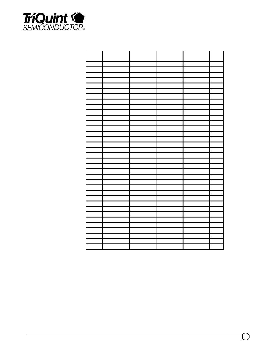
The reference plane for S-parameter data is located at the center of device bond pads.
The S-parameters are also available on floppy disk and the world wide web.
F re quency
S
11
S
21
S
12
S
22
GAIN
(GHz)
MAG
ANG(
o
)
MAG
ANG(
o
)
M AG
ANG(
o
)
MAG
ANG(
o
)
(dB )
0.1
0.40
-46
7.93
0
0.0001
49
0.29
-3
18.0
0.2
0.26
-44
8.29
-1
0.0010
77
0.29
-4
18.4
0.3
0.22
-40
8.39
-7
0.0011
74
0.29
-5
18.5
0.4
0.21
-36
8.42
-12
0.0019
54
0.29
-7
18.5
0.5
0.21
-37
8.45
-16
0.0024
0
0.29
-8
18.5
0.6
0.21
-41
8.47
-20
0.0012
-54
0.30
-10
18.6
0.7
0.19
-41
8.47
-25
0.0003
-14
0.30
-11
18.6
0.8
0.19
-41
8.46
-29
0.0000
64
0.30
-13
18.5
0.9
0.19
-42
8.47
-33
0.0006
107
0.30
-14
18.6
1.0
0.18
-42
8.46
-37
0.0010
107
0.30
-15
18.6
1.1
0.18
-43
8.48
-41
0.0010
98
0.30
-16
18.6
1.2
0.17
-44
8.47
-45
0.0012
111
0.30
-17
18.6
1.3
0.17
-45
8.46
-49
0.0014
101
0.29
-19
18.5
1.4
0.16
-46
8.45
-53
0.0018
105
0.29
-20
18.5
1.5
0.16
-47
8.39
-58
0.0019
102
0.29
-22
18.5
1.6
0.16
-49
8.31
-62
0.0020
108
0.29
-24
18.4
1.7
0.16
-52
8.23
-66
0.0020
105
0.28
-26
18.3
1.8
0.16
-58
8.20
-69
0.0020
104
0.28
-28
18.3
1.9
0.16
-65
8.20
-73
0.0020
108
0.28
-31
18.3
2.0
0.17
-71
8.22
-77
0.0022
108
0.28
-34
18.3
2.1
0.18
-78
8.22
-81
0.0027
105
0.28
-37
18.3
2.2
0.18
-83
8.20
-86
0.0030
107
0.28
-41
18.3
2.3
0.19
-88
8.15
-90
0.0029
106
0.28
-45
18.2
2.4
0.21
-91
8.09
-95
0.0031
107
0.29
-48
18.2
2.5
0.22
-94
8.01
-99
0.0032
107
0.30
-51
18.1
2.6
0.23
-96
7.92
-104
0.0034
111
0.30
-55
18.0
2.7
0.25
-97
7.81
-108
0.0033
109
0.32
-58
17.9
2.8
0.26
-97
7.70
-12
0.0038
105
0.32
-60
17.7
2.9
0.27
-97
7.56
-17
0.0040
107
0.34
-62
17.6
3.0
0.28
-97
7.44
-121
0.0041
104
0.35
-64
17.4
3.1
0.29
-95
7.29
-125
0.0041
107
0.36
-65
17.3
3.2
0.30
-94
7.16
-129
0.0044
109
0.37
-66
17.1
3.3
0.31
-93
7.03
-133
0.0044
107
0.38
-67
16.9
3.4
0.32
-91
6.88
-137
0.0050
106
0.39
-67
16.8
3.5
0.32
-90
6.74
-141
0.0048
109
0.39
-67
16.6
TYPICAL S-PARAMETERS

TriQuint Semiconductor Texas Phone: (972)994 8465 Fax: (972)994 8504 Web: www.triquint.com
Product Data Sheet
5
TGA8061-SCC
RF CHARACTERISTICS
V+ = 12 V, V
O
= 5 V, T
A
= 25
o
C
P ARAMETER
TEST CONDITIONS
TYP
UNIT
I
+
Pos itive s upply current
V
+
= 12 V, V
O
= 5 V, T
A
= 25
o
C
112
mA
DC CHARACTERISTICS
T
A
= 25
o
C
EQUIVALENT
SCHEMATIC
TYPICAL BIAS
NETWORK
Select V
ADJ
to set V
O
= 5 V+/- 0.5 V. Select resistor R1-R4 to set V
D1
= 4.5 V +/- 0.5 V.
P AR AM ETER
TES T C ONDITIONS
TYP
UNIT
1.0 GHz
26
I
P
3
ThirdÙorder intercept
2.0 GHz
25
dBm
3.5 GHz
22
0.1 GHz
15
1.0 GHz
16
P
1dB
1ÙdB gain compres s ion
2.0 GHz
16
dBm
3.0 GHz
14
4.0 GHz
12
TriQuint Semiconductor Texas Phone: (972)994 8465 Fax: (972)994 8504 Web: www.triquint.com
Product Data Sheet
6
TGA8061-SCC
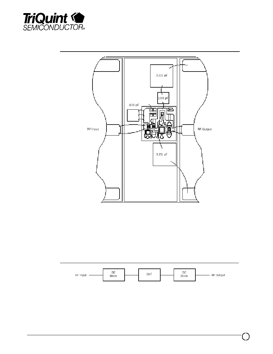
RECOMMENDED
ASSEMBLY DIAGRAM
RECOMMENDED
TEST
CONFIGURATION
Close placement of external components is essential to stability.
V
S1
connections: bond using three 1-mil diameter, 15 to 30-mil-length gold wires for optimum RF performance.
The 100 pF capacitor should be placed within 15-mils of the chip, and source wires to this chip should be kept
as short as possible.

TriQuint Semiconductor Texas Phone: (972)994 8465 Fax: (972)994 8504 Web: www.triquint.com
Product Data Sheet
7
TGA8061-SCC
GaAs MMIC devices are susceptible to damage from Electrostatic Discharge. Proper precautions should be observed
during handling, assembly and test.
MECHANICAL DRAWING