TriQuint Semiconductor Texas Phone: (972)994 8465 Fax: (972)994 8504 Web: www.triquint.com Info:
info-mmw@tqs.com
Advance Product Information
June 3, 2003
1
Note: Devices designated as EPU are typically early in their characterization process prior to finalizing all electrical and process
specifications. Specifications are subject to change without notice.
4 Watt Ka Band Packaged Amplifier
TGA4905-EPU-CP
Key Features and Performance
À
36 dBm Midband Psat
À
22 dB Nominal Gain
À
10 dB Typical Input Return Loss
À
8 dB Typical Output Return Loss
À
25 - 31 GHz Frequency Range
À
0.25Ám pHEMT Technology
À
Bias Conditions: 6 V, 2.1 A (Quiescent)
À
Package Dimensions:
13.34 x 9.65 x 1.85 mm
(0.525 x 0.380 x 0.073 in)
Preliminary Measured Performance
Bias Conditions: Vd=6 V Idq=2.1 A
Primary Applications
À
Satellite Ground Terminals
À
Point to Point
À
LMDS
20
22
24
26
28
30
32
34
36
38
40
24
25
26
27
28
29
30
31
32
Frequency (GHz)
Po
u
t
@
Pi
n
= +18 d
B
m (
d
Bm)
-30
-24
-18
-12
-6
0
6
12
18
24
30
20
22
24
26
28
30
32
34
36
38
40
Frequency (GHz)
Gain (dB)
-30
-24
-18
-12
-6
0
6
12
18
24
30
Return Loss (dB)
Gain
Input
Output
Product Description
The TriQuint TGA4905-EPU-CP is a
compact 4 Watt High Power Amplifier
Packaged MMIC for Ka-band
applications. The part is designed using
TriQuint's proven standard 0.25 um gate
Power pHEMT production process.
The TGA4905 provides a nominal 36
dBm of output power at an input power
level of 18 dBm from 25-31 GHz with a
small signal gain of 22 dB.
The part is ideally suited for low cost
emerging markets such as base station
transmitters for satellite ground terminals,
point to point radio and LMDS.
The TGA4905-EPU-CP is 100% RF
tested to ensure performance
compliance.
TriQuint Semiconductor Texas Phone: (972)994 8465 Fax: (972)994 8504 Web: www.triquint.com Info:
info-mmw@tqs.com
Advance Product Information
June 3, 2003
2
Note: Devices designated as EPU are typically early in their characterization process prior to finalizing all electrical and process
specifications. Specifications are subject to change without notice.
TGA4905-EPU-CP
TABLE I
MAXIMUM RATINGS
Symbol
Parameter 1/
Value
Notes
V
D
Drain Voltage
8 V
2/
V
G
Gate Voltage Range
-5 V to 0 V
I
D
Drain Current (Quiescent)
3.0 A
2/
| I
G
|
Gate Current
62 mA
P
IN
Input Continuous Wave Power
24 dBm
2/
P
D
Power Dissipation
16.8 W
2/ 3/
T
CH
Operating Channel Temperature
150
0
C
4/ 5/
T
M
Mounting Temperature (30 Seconds)
320
0
C
T
STG
Storage Temperature
-65 to 150
0
C
1/
These ratings represent the maximum operable values for this device.
2/
Combinations of supply voltage, supply current, input power, and output power shall not exceed P
D
.
3/
P
D
is the power dissipation allowed in order to reach a channel temperature of 150
░
C with a package
base temperature of 70
░
C. When operated at this power dissipation with a baseplate temperature of
70
░
C, the MTTF is 1.0E+6 hours.
4/
These ratings apply to each individual FET.
5/
Junction operating temperature will directly affect the device median time to failure (T
M
). For
maximum life, it is recommended that junction temperatures be maintained at the lowest possible
levels.

TriQuint Semiconductor Texas Phone: (972)994 8465 Fax: (972)994 8504 Web: www.triquint.com Info:
info-mmw@tqs.com
Advance Product Information
June 3, 2003
3
Note: Devices designated as EPU are typically early in their characterization process prior to finalizing all electrical and process
specifications. Specifications are subject to change without notice.
TABLE II
RF CHARACTERIZATION TABLE
(T
A
= 25
░
C, Nominal)
(Vd = 6 V, Idq = 2.1 A)
SYMBOL
PARAMETER
TEST CONDITION
TYPICAL
UNITS
Gain
Small Signal Gain
F = 25 ¡ 31GHz
22
dB
IRL
Input Return Loss
F = 25 ¡ 31GHz
10
dB
ORL
Output Return Loss
F = 25 ¡ 31GHz
8
dB
PWR
Output Power @ Psat
F = 25 ¡ 31GHz
36
dBm
TABLE III
THERMAL INFORMATION*
Parameter
Test Conditions
T
CH
(
░
C)
R
JC
(
░
C/W)
T
M
(hrs)
R
JC
Thermal Resistance
(Channel to Backside of
Package)
V
D
= 6 V
I
D
= 2.1 A
P
DISS
= 12.6 W
128.35
4.63
6.9 E+6
Note: Carrier at 70
░
C baseplate temperature. Worst case condition with no RF applied,
100% of DC power is dissipated.
* The thermal information is a result of a detailed thermal model
TGA4905-EPU-CP

TriQuint Semiconductor Texas Phone: (972)994 8465 Fax: (972)994 8504 Web: www.triquint.com Info:
info-mmw@tqs.com
Advance Product Information
June 3, 2003
4
Note: Devices designated as EPU are typically early in their characterization process prior to finalizing all electrical and process
specifications. Specifications are subject to change without notice.
Measured Fixtured Performance
V
D
= 6 V Idq = 2.1 A
TGA4905-EPU-CP
-30
-24
-18
-12
-6
0
6
12
18
24
30
20
22
24
26
28
30
32
34
36
38
40
Frequency (GHz)
Gai
n
(dB)
-30
-24
-18
-12
-6
0
6
12
18
24
30
Return Loss (dB)
Gain
Input
Output
20
22
24
26
28
30
32
34
36
38
40
24
25
26
27
28
29
30
31
32
Frequency (GHz)
Pout @ Pin = +18 dBm (dBm)
TriQuint Semiconductor Texas Phone: (972)994 8465 Fax: (972)994 8504 Web: www.triquint.com Info:
info-mmw@tqs.com
Advance Product Information
June 3, 2003
5
Note: Devices designated as EPU are typically early in their characterization process prior to finalizing all electrical and process
specifications. Specifications are subject to change without notice.
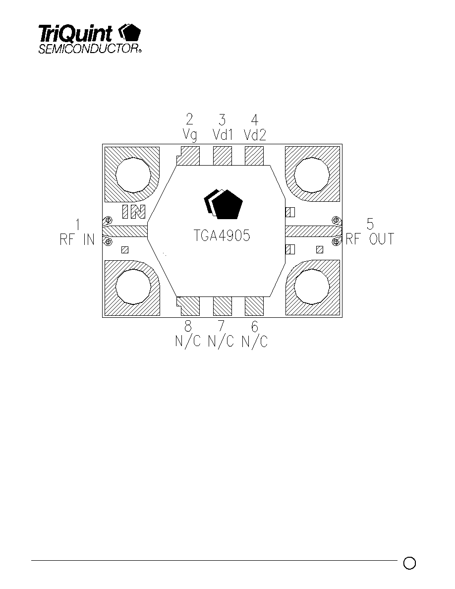
Package Pinout Diagram
GaAs MMIC devices are susceptible to damage from Electrostatic Discharge. Proper precautions should
be observed during handling, assembly and test.
TGA4905-EPU-CP