1
Note: Devices designated as EPU are typically early in their characterization process prior to finalizing all electrical and process
specifications. Specifications are subject to change without notice
TriQuint Semiconductor Texas Phone: (972)994-8465 Fax: (972)994-8504 Email: info-mmw@tqs.com Web: www.triquint.com
Advance Product Information
July 22, 2004
12.5Gb/s Modulator Driver Amplifier
TGA4802-EPU
Metro and Long Haul Applications
Key Features and Performance
Ę
Frequency Range: DC - 25 GHz
Ę
Single-ended Input / Output
Ę
15 dB Small Signal Gain
Ę
18 GHz Small Signal Bandwidth
Ę
Wide Drive Range (3V to 7V)
Ę
15ps Edge Rates (20/80)
Ę
Power Dissipation 1.2 Watts
Ę
0.25um pHEMT 2MI Technology
Ę
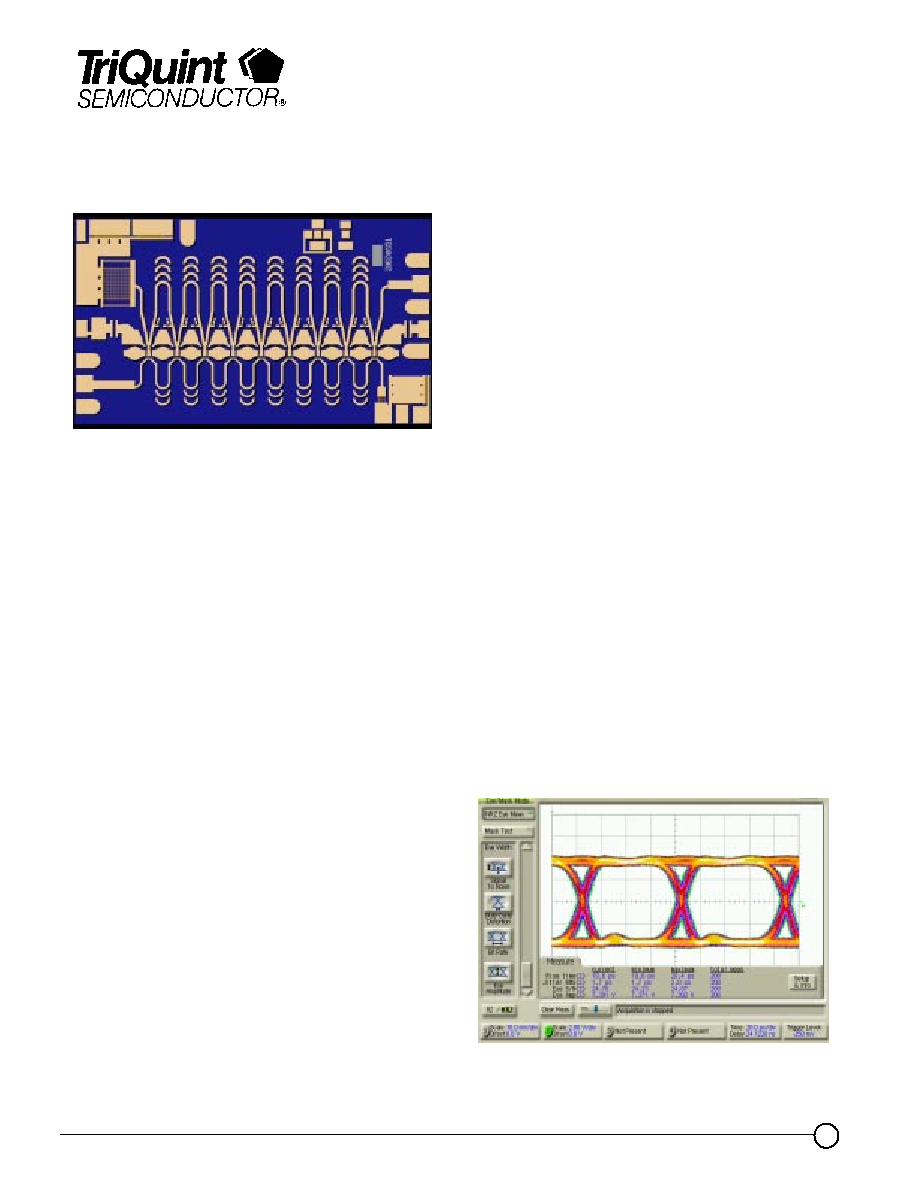
Die Size: 3.3 x 2.0 x 0.1 mm
(0.131 x 0.79 x 0.004 inches)
Primary Applications
Ę
Mach-Zehnder Modulator Driver for
Metro and Long Haul
Description
The TriQuint TGA4802 is part of a series of optical driver
amplifiers suitable for a variety of driver applications.
The TGA4802 is a medium power wideband AGC
amplifier MMIC die that typically provides 15dB small
signal gain with 10dB AGC range. RF ports are DC
coupled enabling the user to customize system corner
frequencies.
The TGA4802 is an excellent choice for 12.5Gb/s optical
modulator driver applications. The TGA4802 has
demonstrated capability to amplify a 2V input signal to
7Vpp saturated.
The TGA4802 requires off-chip decoupling, a DC block
and a bias tee. The TGA4802 is available in die form.
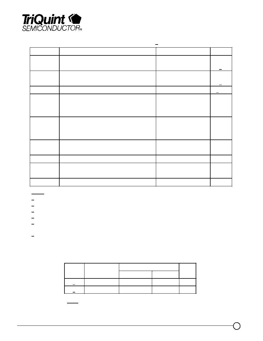
TGA4802 Fixtured Data
Vd(Rfout)=6V, Id=170mA, (Pdc=1.2W)
Vout=7Vpp, Vin = 2Vpp
Scale: 2V/div, 20ps/div
Measured Performance
Vin=2V
12.5Gb/s
Vout=7Vpp
2
Note: Devices designated as EPU are typically early in their characterization process prior to finalizing all electrical and process
specifications. Specifications are subject to change without notice
TriQuint Semiconductor Texas Phone: (972)994-8465 Fax: (972)994-8504 Email: info-mmw@tqs.com Web: www.triquint.com
Advance Product Information
July 22, 2004
TABLE I
MAXIMUM RATINGS 1/
SYMBOL
PARAMETER
VALUE
NOTES
Vd
POSITIVE SUPPLY VOLTAGE
Drain Voltage at RF output
7 V
2/
Id
POSITIVE SUPPLY CURRENT
Drain Current
200 mA
2/
P
d
POWER DISSIPATION
1.4 W
2/, 3/
Vg
Ig
NEGATIVE GATE
Voltage
Gate Current
0 V to Ł3 V
5 mA
Vctrl
Ictrl
CONTROL GATE
Voltage
Gate Current
Vd/2 to Ł3 V
5 mA
4/
P
IN
RF INPUT
Sinusoidal Continuous Wave Power
23 dBm
T
CH
OPERATING CHANNEL TEMPERATURE
150
0
C
5/, 6/
T
M
MOUNTING TEMPERATURE
(30 SECONDS)
320
0
C
T
STG
STORAGE TEMPERATURE
-65 to 150
0
C
TGA4802EPU
Notes:
1/ These ratings represent the maximum operable values for the device.
2/ Assure the combination of Vd and Id does not exceed maximum power dissipation rating.
3/ Assure Vctrl never exceeds Vd during bias on and off sequences, and normal operation.
4/ When operated at this bias condition with a base plate temperature of 70
0
C, the median life is reduced.
5/ Junction operating temperature will directly affect the device median time to failure (MTTF). For
maximum life, it is recommended that junction temperatures be maintained at the lowest possible levels.
6/ These ratings apply to each individual FET.
TABLE II
DC PROBE TEST
(TA = 25
░
C, nominal)
LIMITS
NOTES
SYMBOL
MIN
MAX
UNITS
1/
|V
BVGS
|
11
30
V
1/
|V
BVGD
|
11
30
V
Notes:
1 V
BVGS
and V
BVDS
are negative.
3
Note: Devices designated as EPU are typically early in their characterization process prior to finalizing all electrical and process
specifications. Specifications are subject to change without notice
TriQuint Semiconductor Texas Phone: (972)994-8465 Fax: (972)994-8504 Email: info-mmw@tqs.com Web: www.triquint.com
Advance Product Information
July 22, 2004
Notes:
1/ RF Probe Bias: V
+
= 8 V, adjust Vg1 to achieve Id = 80 mA, Vctrl = +1.5 V
2/ Verified by design, TGA4802 assembled onto an evaluation platform as shown on page 9 then tested
using the application circuit and bias procedure detailed on pages 7 and 8.
3/ Vin = 2 V, Data Rate = 12.5 Gb/s, Vctrl and Vg are adjusted for maximum output.
4/ Computed using RSS Method where Jpp_additive = SQRT(Jpp_out
2
- Jpp_in
2
)
TGA4802EPU
TABLE III
RF SPECIFICATIONS
(T
A
= 25
░
C Nominal)
Bias Conditions: Vd = 7V Id = 170 mA
NOTE
TEST
MEASUREMENT
CONDITIONS
VALUE
UNITS
MIN
TYP
MAX
SMALL SIGNAL BW
18
GHz
1/
SMALL-SIGNAL
GAIN MAGNITUDE
2 - 10 GHz
12 - 18 GHz
14
10
dB
1/
INPUT RETURN LOSS
MAGNITUDE
2 - 14 GHz
10
dB
1/
OUTPUT RETURN LOSS
MAGNITUDE
2 - 14 GHz
12
dB
2/ 3/
SATURATED OUTPUT
POWER
2 - 12 GHz
22
dBm
2/, 3/
EYE AMPLITUDE
Vd(RFout) = 6V
Vd(RFout) = 5V
Vd(RFout) = 4V
7.0
6.0
5.0
Vpp
2/, 4/
ADDITIVE JITTER
5
ps
2/, 4/
RISE TIME (20/80)
15
ps

4
Note: Devices designated as EPU are typically early in their characterization process prior to finalizing all electrical and process
specifications. Specifications are subject to change without notice
TriQuint Semiconductor Texas Phone: (972)994-8465 Fax: (972)994-8504 Email: info-mmw@tqs.com Web: www.triquint.com
Advance Product Information
July 22, 2004
TGA4802EPU
TABLE IV
THERMAL INFORMATION*
PARAMETER
TEST
CONDITIONS
T
CH
(
o
C)
R
T
JC
(
q
C/W)
T
M
(HRS)
R
JC
Thermal Resistance
(channel to backside of
carrier)
Vd (RF out) = 7 V
I
D
= 170 mA
Pdiss = 1.2 W
110
32.7
4.2 E+7
Note: Assumes eutectic attach using 1.5 mil 80/20 AuSn mounted to a 20 mil CuMo Carrier
at 70
░
C baseplate temperature. Worst case condition with no RF applied, 100% of DC
power is dissipated. Thermal transfer is conducted thru the bottom of the TGA4802
into the mounting carrier. Design the mounting interface to assure adequate thermal
transfer to the base plate.
5
Note: Devices designated as EPU are typically early in their characterization process prior to finalizing all electrical and process
specifications. Specifications are subject to change without notice
TriQuint Semiconductor Texas Phone: (972)994-8465 Fax: (972)994-8504 Email: info-mmw@tqs.com Web: www.triquint.com
Advance Product Information
July 22, 2004
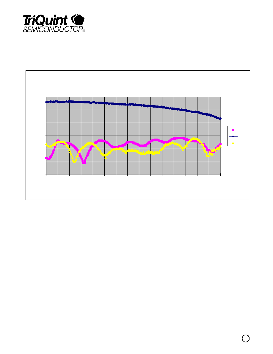
TGA4802EPU - Fixtured Data
Cable Cal - Includes Fixture Losses
-40
-30
-20
-10
0
10
20
0.045
2.043
4.041
6.04
8.038
10.04
12.03
14.03
16.03
18.03
20.03
22.03
24.02
26.02
28.02
30.02
Frequency (GHz)
Gain and RL
IRL
Gain
ORL
TGA4802EPU
Measured Fixtured Data
Bias Conditions: Vd = 7V, Id= 170mA