TriQuint Semiconductor Texas: Phone (972)994-8465 Fax (972)994-8504 Email: Info-mmw@tqs.com Web: www.triquint.com
Advance Product Information
January 17, 2005
1
Note: Devices designated as EPU are typically early in their characterization process prior to finalizing all electrical and process specifications.
Specifications are subject to change without notice
18
20
22
24
26
28
30
32
34
36
38
40
42
44
46
48
Frequency (GHz)
O
u
tput
P
o
w
e
r
(dB
m
)
-30
-25
-20
-15
-10
-5
0
5
10
15
20
32
34
36
38
40
42
44
46
48
Frequency (GHz)
S-p
a
ra
m
e
te
r (d
B)
33 - 47 GHz Wide Band Driver Amplifier TGA4522-EPU
Key Features
�
Frequency Range: 33 - 47 GHz
�
27 dBm Nominal Psat @ 38GHz
�
26 dBm P1dB @ 38 GHz
�
35 dBm OTOI @ Pin = 18 dBm/Tone
�
14 dB Nominal Gain @ 38GHz
�
14 dB Nominal Return Loss @ 38GHz
�
Bias: 6 V @ 400 mA Idq
�
0.25 um 3MI pHEMT Technology
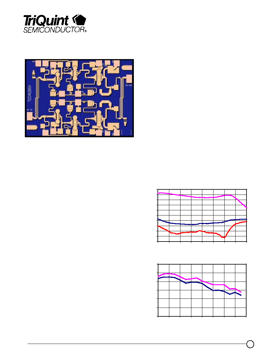
�
Chip Dimensions 2.00 x 1.45 x 0.10 mm
(0.079 x 0.057 x 0.004 in)
Primary Applications
�
Digital Radio
�
Point-to-Point Radio
�
Point-to-Multipoint Communications
�
Military SAT-COM
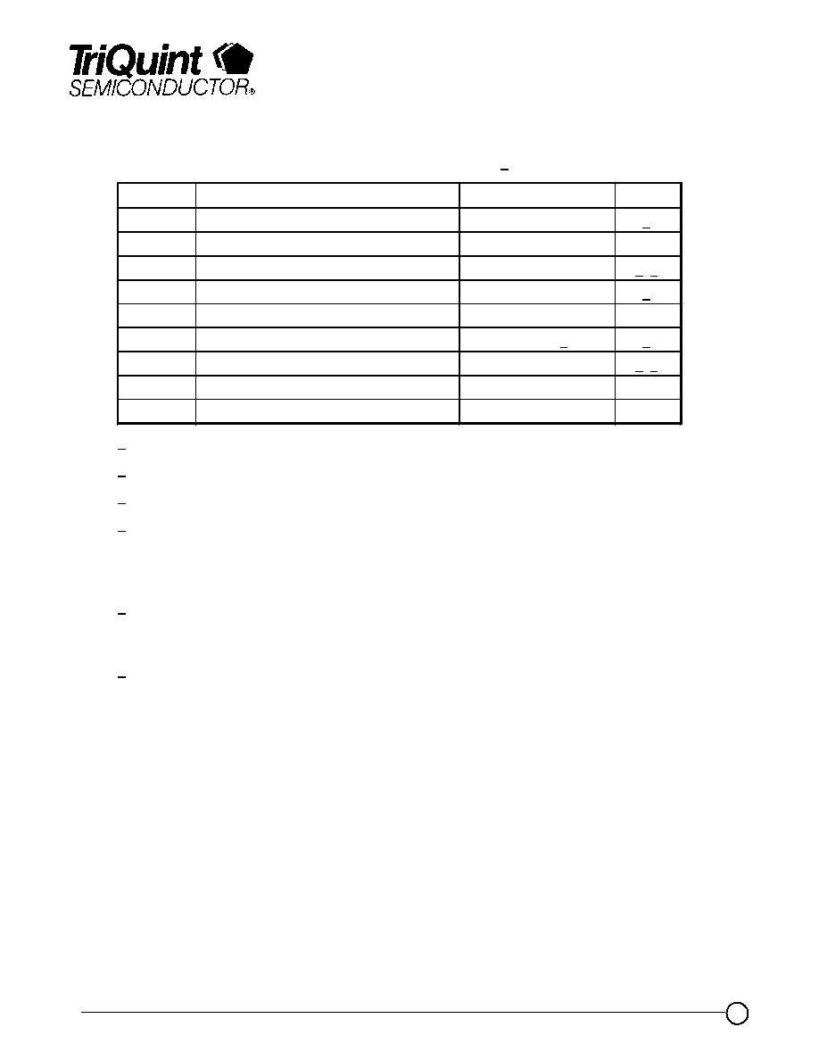
Measured Fixtured Data
Bias Conditions: Vd = 6 V, Idq = 400 mA
Product Description
The TriQuint TGA4522-EPU is a compact Driver
Amplifier MMIC for Ka-band and Q-band
applications. The part is designed using TriQuint's
proven standard 0.25um power pHEMT production
process.
The TGA4522-EPU nominally provides 27 dBm
saturated output power, and 26 dBm output power
at 1dB Gain compression @ 38 GHz. It also has
typical gain of 14 dB, and return loss of 12 dB.
The part is ideally suited for low cost emerging
markets such as Digital Radio, Point-to-Point
Radio and Point-to-Multi Point Communications.
The TGA4522-EPU is 100% DC and RF tested on-
wafer to ensure performance compliance.
Gain
IRL
ORL
Psat
P1dB
TriQuint Semiconductor Texas: Phone (972)994-8465 Fax (972)994-8504 Email: Info-mmw@tqs.com Web: www.triquint.com
Advance Product Information
January 17, 2005
2
Note: Devices designated as EPU are typically early in their characterization process prior to finalizing all electrical and process specifications.
Specifications are subject to change without notice
TABLE I
MAXIMUM RATINGS 1/
SYMBOL
PARAMETER
VALUE
NOTES
Vd
Drain Voltage
8 V
2/
Vg
Gate Voltage Range
-2 TO 0 V
Id
Drain Current
700 mA
2/ 3/
Ig
Gate Current
16 mA
3/
P
IN
Input Continuous Wave Power
23 dBm
P
D
Power Dissipation
See note 4/
2/
T
CH
Operating Channel Temperature
150
0
C
5/ 6/
T
M
Mounting Temperature (30 Seconds)
320
0
C
T
STG
Storage Temperature
-65 to 150
0
C
1/
These ratings represent the maximum operable values for this device.
2/
Combinations of supply voltage, supply current, input power, and output power shall not exceed P
D
.
3/
Total current for the entire MMIC.
4/
For a median life time of 1E+6 hrs, Power dissipation is limited to:
P
D
(max) = (150
0
C � T
BASE
0
C) / 35.5 (
0
C/W)
Where T
BASE
is the base plate temperature.
5/
Junction operating temperature will directly affect the device median time to failure (MTTF). For
maximum life, it is recommended that junction temperatures be maintained at the lowest possible
levels.
6/
These ratings apply to each individual FET.
TGA4522-EPU
TriQuint Semiconductor Texas: Phone (972)994-8465 Fax (972)994-8504 Email: Info-mmw@tqs.com Web: www.triquint.com
Advance Product Information
January 17, 2005
3
Note: Devices designated as EPU are typically early in their characterization process prior to finalizing all electrical and process specifications.
Specifications are subject to change without notice
TABLE II
ELECTRICAL CHARACTERISTICS
(Ta = 25
0
C Nominal)
TGA4522-EPU
PARAMETER
TYPICAL
UNITS
Frequency Range
33 - 47
GHz
Drain Voltage, Vd
6.0
V
Drain Current, Id
400
mA
Gate Voltage, Vg
-0.5
V
Small Signal Gain, S21
13
dB
Input Return Loss, S11
14
dB
Output Return Loss, S22
18
dB
Output Power @ 1dB Gain Compression, P1dB
26
dBm
Saturated Power, Psat
27
dBm
TABLE III
THERMAL INFORMATION
PARAMETER
TEST CONDITIONS
T
CH
(
O
C)
R
T
JC
(
q
C/W)
T
M
(HRS)
R
JC
Thermal Resistance
(channel to Case)
Vd = 5 V
Id = 400 mA
Pdiss = 2.0 W
140
35.5
2.4E+6
Note: Assumes eutectic attach using 1.5 mil 80/20 AuSn mounted to a 20 mil CuMo
Carrier at 50
o
C baseplate temperature. Worst case condition with no RF applied, 100%
of DC power is dissipated.
TriQuint Semiconductor Texas: Phone (972)994-8465 Fax (972)994-8504 Email: Info-mmw@tqs.com Web: www.triquint.com
Advance Product Information
January 17, 2005
4
Note: Devices designated as EPU are typically early in their characterization process prior to finalizing all electrical and process specifications.
Specifications are subject to change without notice
-30
-25
-20
-15
-10
-5
0
5
10
15
20
30
32
34
36
38
40
42
44
46
48
50
Frequency (GHz)
R
e
tu
r
n
L
o
s
s
(d
B
)
0
2
4
6
8
10
12
14
16
18
20
30
32
34
36
38
40
42
44
46
48
50
Frequency (GHz)
Ga
i
n
(
d
B
)
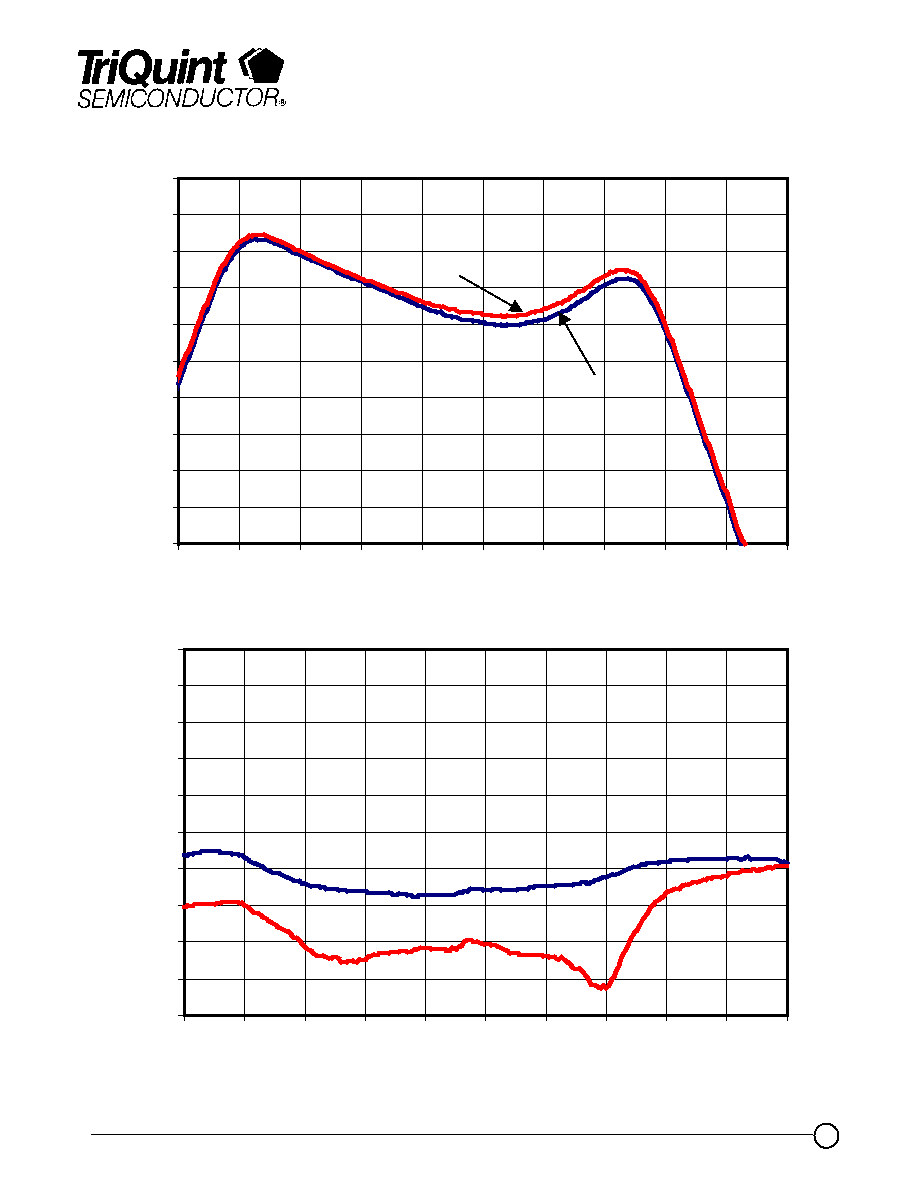
TGA4522-EPU
Preliminary Measured Data
Bias Conditions: Vd = 5-6 V, Idq = 400 mA
IRL
ORL
6V
5V
Bias Conditions: Vd = 6 V, Idq = 400 mA
TriQuint Semiconductor Texas: Phone (972)994-8465 Fax (972)994-8504 Email: Info-mmw@tqs.com Web: www.triquint.com
Advance Product Information
January 17, 2005
5
Note: Devices designated as EPU are typically early in their characterization process prior to finalizing all electrical and process specifications.
Specifications are subject to change without notice
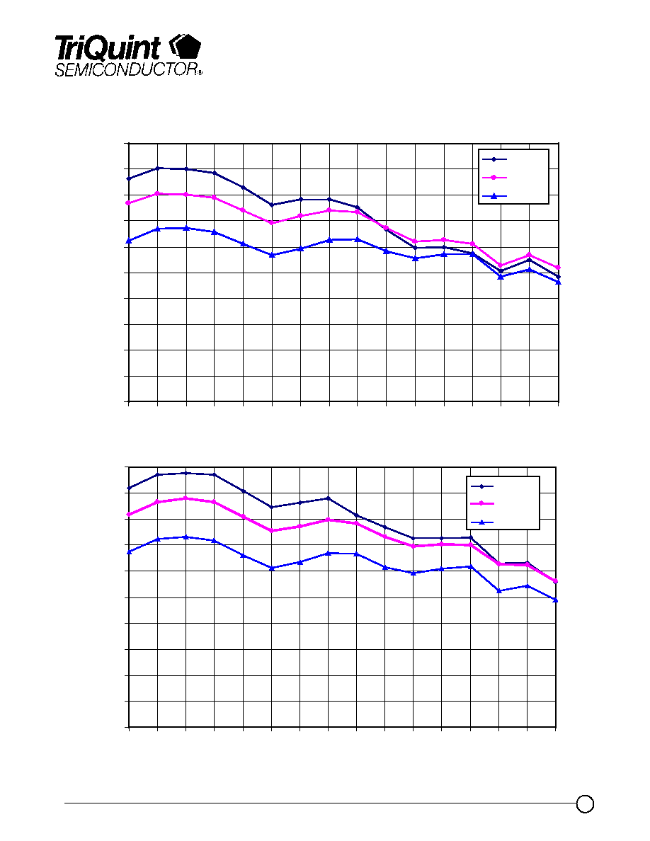
TGA4522-EPU
Preliminary Measured Data
Bias Conditions: Vd = 4 - 6 V, Idq = 400 mA
18
19
20
21
22
23
24
25
26
27
28
32
33
34
35
36
37
38
39
40
41
42
43
44
45
46
47
Frequency (GHz)
P
1
d
B
(
dBm
)
Vd=6V
Vd=5V
Vd=4V
18
19
20
21
22
23
24
25
26
27
28
32
33
34
35
36
37
38
39
40
41
42
43
44
45
46
47
Frequency (GHz)
P
sat
(
d
B
m
)
Vd=6V
Vd=5V
Vd=4V