TriQuint Semiconductor Texas: Phone (972)994-8465 Fax (972)994 8504 Web: www.triquint.com
Advance Product Information
August 5, 2002
1
Note: Devices designated as EPU are typically early in their characterization process prior to finalizing all electrical and process
specifications. Specifications are subject to change without notice.
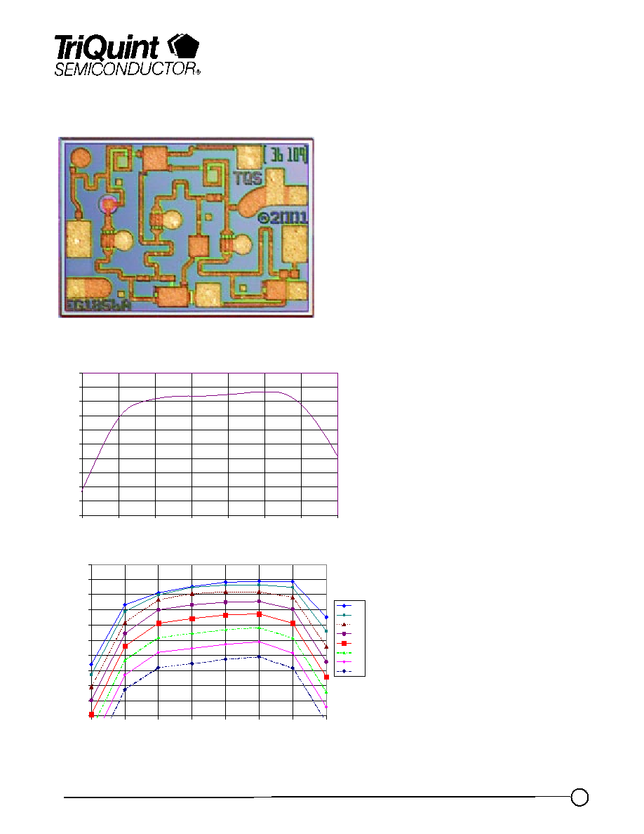
29-37 GHz Compact Driver Amplifier
TGA4510-EPU
Key Features
ñ
0.25 um pHEMT Technology
ñ
>16 dB Nominal Gain @ 30 GHz
ñ
16 dBm Nominal Psat
ñ
Bias Conditions: Vd = 6V, Id = 60 mA
ñ
Compact Chip Size: 1.1 x 0.8 x 0.1 mm
3
Primary Applications
ñ
LMDS
ñ
Point-to-Point
ñ
Base Stations
Fixtured Measured Performance
Bias Conditions: Vd = 6V, Id = 60 mA Ý 5%
0
2
4
6
8
10
12
14
16
18
20
26
28
30
32
34
36
38
40
Frequency (GHz)
Gai
n
(dB)
,
0
2
4
6
8
10
12
14
16
18
20
26
28
30
32
34
36
38
40
Frequency (GHz)
P
out
(
d
B
m
)
4
2
0
-2
-4
-6
-8
-10
Pwr(in)
TriQuint Semiconductor Texas: Phone (972)994-8465 Fax (972)994 8504 Web: www.triquint.com
Advance Product Information
August 5, 2002
2
Note: Devices designated as EPU are typically early in their characterization process prior to finalizing all electrical and process
specifications. Specifications are subject to change without notice.
TGA4510-EPU
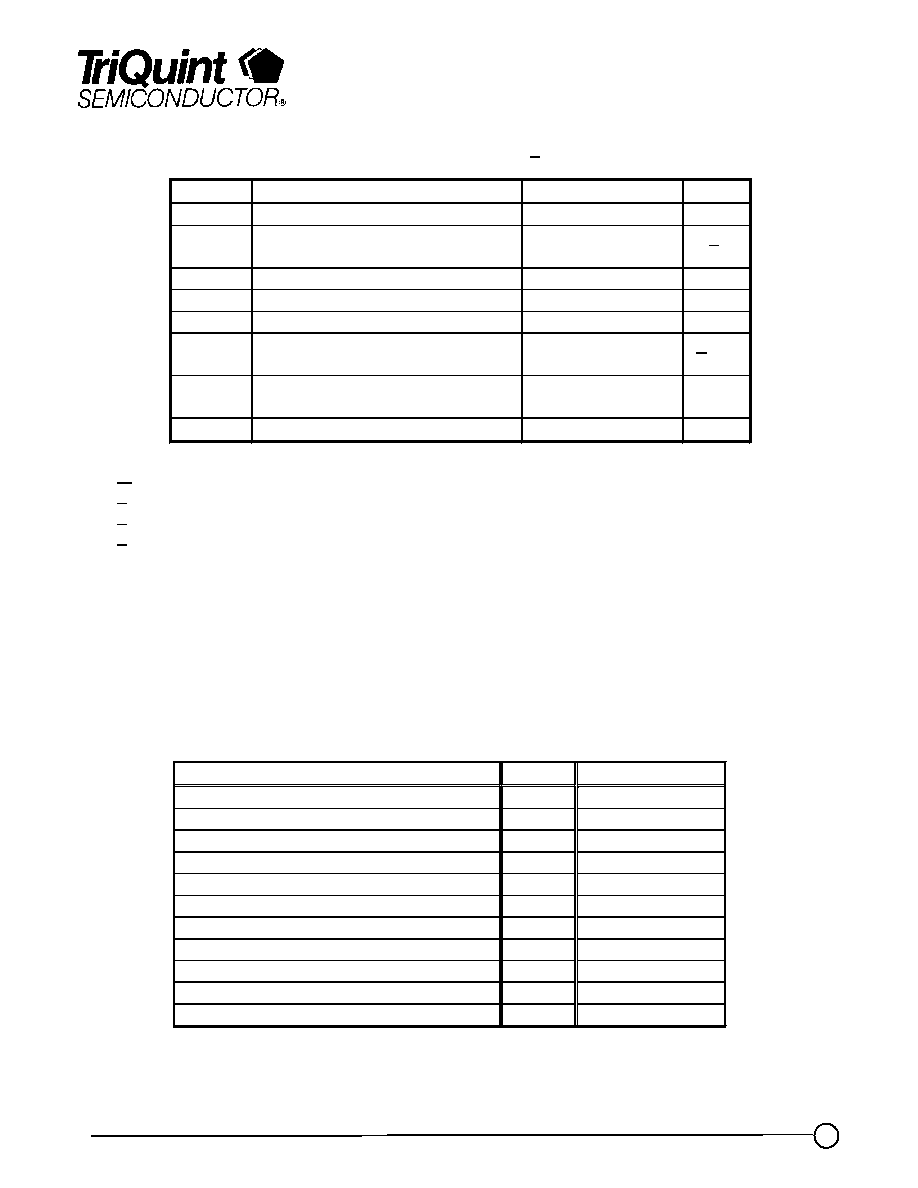
TABLE II
ELECTRICAL CHARACTERISTICS
(Ta = 25
o
C Ý 5
o
C)
TABLE I
MAXIMUM RATINGS 1/
Symbol
Parameter
Value
Notes
V
+
Positive Supply Voltage
8V
I
+
Positive Supply Current
(Quiescent)
81mA
2/
|I
G
|
Gate Current
3.5 mA
P
D
Power Dissipation
TBD
P
IN
Input Continuous Wave Power
18 dBm
T
CH
Operating Channel
Temperature
150
¯
C
3/, 4/
T
M
Mounting Temperature (30
seconds)
320
¯
C
T
STG
Storage Temperature
-65
¯
C to 150
¯
C
1/
These values represent the maximum operable values of this device
2/
Total current for the entire MMIC
3/
These ratings apply to each individual FET
4/
Junction operating temperature will directly affect the device mean time to
failure (MTTF). For maximum life it is recommended that junction
temperatures be maintained at the lowest possible levels.
Parameter
Units
Typical
Frequency Band
GHz
29 - 37
Drain Operating Voltage
V
6
Gate Operating Voltage
V
-0.6
Drain Current, Quiescent
mA
60
Typical DC Power Consumption
W
0.36
Small Signal Gain
dB
15.8 Ù 17.6
Gain Flatness
dB
< 0.05
Input Return Loss
dB
> 8
Output Return Loss
dB
> 11
TOI (Single Tone Power) @ 30 GHz
dBm
22
CW Output Power @ P1dB (dBm)
dBm
14.0 Ù 16.2
TriQuint Semiconductor Texas: Phone (972)994-8465 Fax (972)994 8504 Web: www.triquint.com
Advance Product Information
August 5, 2002
3
Note: Devices designated as EPU are typically early in their characterization process prior to finalizing all electrical and process
specifications. Specifications are subject to change without notice.
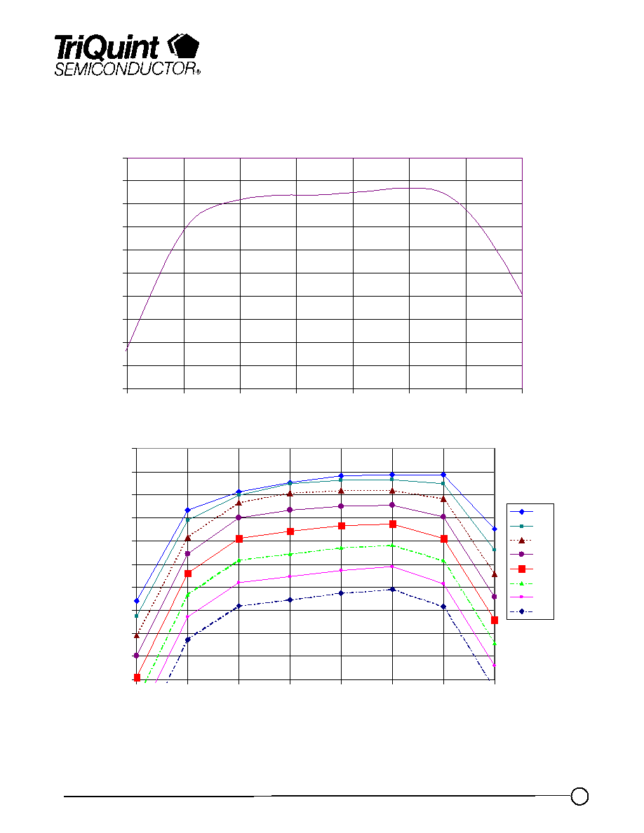
TGA4510-EPU
,
0
2
4
6
8
10
12
14
16
18
20
26
28
30
32
34
36
38
40
Frequency (GHz)
P
o
ut (
d
B
m
)
4
2
0
-2
-4
-6
-8
-10
Pwr(in)
Note: Pwr (in) = 0dBm is approximately P1dB (dbM)
Bias Conditions: Vd = 6V, Id = 60mA Ý 5%
Measured Fixtured Data
0
2
4
6
8
10
12
14
16
18
20
26
28
30
32
34
36
38
40
Frequency (GHz)
Gain (dB)
TriQuint Semiconductor Texas: Phone (972)994-8465 Fax (972)994 8504 Web: www.triquint.com
Advance Product Information
August 5, 2002
4
Note: Devices designated as EPU are typically early in their characterization process prior to finalizing all electrical and process
specifications. Specifications are subject to change without notice.
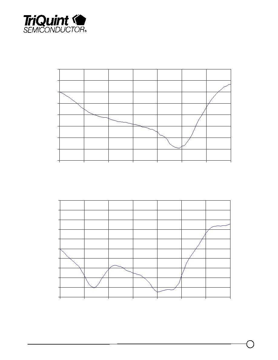
Measured Fixtured Data
TGA4510-EPU
Bias Conditions: Vd = 6V, Id = 60mA Ý 5%
-16
-14
-12
-10
-8
-6
-4
-2
0
26
28
30
32
34
36
38
40
Frequency (GHz)
Input Return Loss (dB)
-20
-18
-16
-14
-12
-10
-8
-6
-4
-2
0
26
28
30
32
34
36
38
40
Frequency (GHz)
O
u
tput R
e
turn Loss (dB
)
TriQuint Semiconductor Texas: Phone (972)994-8465 Fax (972)994 8504 Web: www.triquint.com
Advance Product Information
August 5, 2002
5
Note: Devices designated as EPU are typically early in their characterization process prior to finalizing all electrical and process
specifications. Specifications are subject to change without notice.
TGA4510-EPU
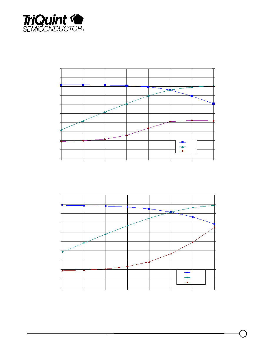
Measured Fixtured Data
Bias Conditions: Vd = 6V, Id = 60 mA Ý 5%, @ 30 GHz
0
2
4
6
8
10
12
14
16
18
20
-10
-8
-6
-4
-2
0
2
4
Pin (dBm)
Gain (dB),Pout (dBm
)
50
55
60
65
70
75
80
85
90
95
100
Id (m
A)
Gain
Pout
Id
Bias Conditions: Vd = 6V, Id = 60 mA Ý 5%, @ 36 GHz
0
2
4
6
8
10
12
14
16
18
20
-10
-8
-6
-4
-2
0
2
4
Pin (dBm)
Gain (dB),Pout (dBm)
50
55
60
65
70
75
80
85
90
95
100
Id (mA)
Gain
Pout
Id